当前位置:
X-MOL 学术
›
Acta Mater.
›
论文详情
Our official English website, www.x-mol.net, welcomes your feedback! (Note: you will need to create a separate account there.)
Domain engineering of epitaxial (001) Bi2Te3 thin films by miscut GaAs substrate
Acta Materialia ( IF 9.4 ) Pub Date : 2020-09-01 , DOI: 10.1016/j.actamat.2020.07.051 Kwang-Chon Kim , Seong Keun Kim , Jin-Sang Kim , Seung-Hyub Baek
Acta Materialia ( IF 9.4 ) Pub Date : 2020-09-01 , DOI: 10.1016/j.actamat.2020.07.051 Kwang-Chon Kim , Seong Keun Kim , Jin-Sang Kim , Seung-Hyub Baek
|
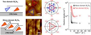
Abstract Herein, we have reported domain engineering of epitaxial (001) Bi2Te3 thin films by miscut (100) substrates. On a nominal flat (100) GaAs substrate, two-variant domains that were in-plane rotated by 60°, including the 60° domain boundaries, were formed in the epitaxial Bi2Te3 film, such that the symmetry elements of two-fold rotational and/or mirror symmetries of the GaAs substrate were preserved. The domain variants were successfully reduced to obtain mono-domain Bi2Te3 thin films without any domain boundaries using the 2°-miscut GaAs substrates, where a particular step-and-terrace structure on the vicinal surface macroscopically broke the intrinsic symmetry of GaAs, lowering the number of possible domains. Depending on the miscut directions, the in-plane orientations of the mono-domain Bi2Te3 films were varied with respect to the GaAs substrate. A model was proposed to explain the effect of miscut substrate on the domain structure of Bi2Te3 thin films. Low-temperature Hall measurements revealed that in the intrinsic regime (10 K) the electron concentration of the mono-domain Bi2Te3 films (~2 × 1018 cm−3) was significantly lower than that of the two-domain films (~1019 cm−3). This was attributed to the donor-like effect of the 60° domain boundaries. These results provide an opportunity not only to integrate the single-crystalline, mono-domain, layered-chalcogenides on semiconductor single crystals, but also to manipulate their electronic transport properties by domain engineering.
中文翻译:

通过错切 GaAs 衬底进行外延 (001) Bi2Te3 薄膜的域工程
摘要在此,我们报道了通过错切 (100) 衬底进行外延 (001) Bi2Te3 薄膜的域工程。在标称的平面 (100) GaAs 衬底上,在外延 Bi2Te3 薄膜中形成了面内旋转 60° 的两个变体域,包括 60° 域边界,使得二次旋转的对称元素和/ 或 GaAs 衬底的镜像对称性得以保留。使用 2° 错切 GaAs 衬底成功地减少了域变体以获得没有任何域边界的单域 Bi2Te3 薄膜,其中邻近表面上的特定阶梯和平台结构在宏观上破坏了 GaAs 的内在对称性,降低了可能的域数。根据错切方向,单畴 Bi2Te3 薄膜的面内取向相对于 GaAs 衬底是不同的。提出了一个模型来解释错切衬底对 Bi2Te3 薄膜畴结构的影响。低温霍尔测量表明,在本征状态(10 K)中,单畴 Bi2Te3 薄膜(~2 × 1018 cm-3)的电子浓度显着低于双畴薄膜(~1019 cm-)的电子浓度。 3)。这归因于 60° 域边界的类施主效应。这些结果不仅提供了将单晶、单畴、层状硫属化物集成到半导体单晶上的机会,而且还提供了通过畴工程操纵它们的电子传输特性的机会。提出了一个模型来解释错切衬底对 Bi2Te3 薄膜畴结构的影响。低温霍尔测量表明,在本征状态(10 K)中,单畴 Bi2Te3 薄膜(~2 × 1018 cm-3)的电子浓度显着低于双畴薄膜(~1019 cm-)的电子浓度。 3)。这归因于 60° 域边界的类施主效应。这些结果不仅提供了将单晶、单畴、层状硫属化物集成到半导体单晶上的机会,而且还提供了通过畴工程操纵它们的电子传输特性的机会。提出了一个模型来解释错切衬底对 Bi2Te3 薄膜畴结构的影响。低温霍尔测量表明,在本征状态(10 K)中,单畴 Bi2Te3 薄膜(~2 × 1018 cm-3)的电子浓度显着低于双畴薄膜(~1019 cm-)的电子浓度。 3)。这归因于 60° 域边界的类施主效应。这些结果不仅提供了将单晶、单畴、层状硫属化物集成到半导体单晶上的机会,而且还提供了通过畴工程操纵它们的电子传输特性的机会。低温霍尔测量表明,在本征状态(10 K)中,单畴 Bi2Te3 薄膜(~2 × 1018 cm-3)的电子浓度显着低于双畴薄膜(~1019 cm-)的电子浓度。 3)。这归因于 60° 域边界的类施主效应。这些结果不仅提供了将单晶、单畴、层状硫属化物集成到半导体单晶上的机会,而且还提供了通过畴工程操纵它们的电子传输特性的机会。低温霍尔测量表明,在本征状态(10 K)中,单畴 Bi2Te3 薄膜(~2 × 1018 cm-3)的电子浓度显着低于双畴薄膜(~1019 cm-)的电子浓度。 3)。这归因于 60° 域边界的类施主效应。这些结果不仅提供了将单晶、单畴、层状硫属化物集成到半导体单晶上的机会,而且还提供了通过畴工程操纵它们的电子传输特性的机会。
更新日期:2020-09-01
中文翻译:
通过错切 GaAs 衬底进行外延 (001) Bi2Te3 薄膜的域工程
摘要在此,我们报道了通过错切 (100) 衬底进行外延 (001) Bi2Te3 薄膜的域工程。在标称的平面 (100) GaAs 衬底上,在外延 Bi2Te3 薄膜中形成了面内旋转 60° 的两个变体域,包括 60° 域边界,使得二次旋转的对称元素和/ 或 GaAs 衬底的镜像对称性得以保留。使用 2° 错切 GaAs 衬底成功地减少了域变体以获得没有任何域边界的单域 Bi2Te3 薄膜,其中邻近表面上的特定阶梯和平台结构在宏观上破坏了 GaAs 的内在对称性,降低了可能的域数。根据错切方向,单畴 Bi2Te3 薄膜的面内取向相对于 GaAs 衬底是不同的。提出了一个模型来解释错切衬底对 Bi2Te3 薄膜畴结构的影响。低温霍尔测量表明,在本征状态(10 K)中,单畴 Bi2Te3 薄膜(~2 × 1018 cm-3)的电子浓度显着低于双畴薄膜(~1019 cm-)的电子浓度。 3)。这归因于 60° 域边界的类施主效应。这些结果不仅提供了将单晶、单畴、层状硫属化物集成到半导体单晶上的机会,而且还提供了通过畴工程操纵它们的电子传输特性的机会。提出了一个模型来解释错切衬底对 Bi2Te3 薄膜畴结构的影响。低温霍尔测量表明,在本征状态(10 K)中,单畴 Bi2Te3 薄膜(~2 × 1018 cm-3)的电子浓度显着低于双畴薄膜(~1019 cm-)的电子浓度。 3)。这归因于 60° 域边界的类施主效应。这些结果不仅提供了将单晶、单畴、层状硫属化物集成到半导体单晶上的机会,而且还提供了通过畴工程操纵它们的电子传输特性的机会。提出了一个模型来解释错切衬底对 Bi2Te3 薄膜畴结构的影响。低温霍尔测量表明,在本征状态(10 K)中,单畴 Bi2Te3 薄膜(~2 × 1018 cm-3)的电子浓度显着低于双畴薄膜(~1019 cm-)的电子浓度。 3)。这归因于 60° 域边界的类施主效应。这些结果不仅提供了将单晶、单畴、层状硫属化物集成到半导体单晶上的机会,而且还提供了通过畴工程操纵它们的电子传输特性的机会。低温霍尔测量表明,在本征状态(10 K)中,单畴 Bi2Te3 薄膜(~2 × 1018 cm-3)的电子浓度显着低于双畴薄膜(~1019 cm-)的电子浓度。 3)。这归因于 60° 域边界的类施主效应。这些结果不仅提供了将单晶、单畴、层状硫属化物集成到半导体单晶上的机会,而且还提供了通过畴工程操纵它们的电子传输特性的机会。低温霍尔测量表明,在本征状态(10 K)中,单畴 Bi2Te3 薄膜(~2 × 1018 cm-3)的电子浓度显着低于双畴薄膜(~1019 cm-)的电子浓度。 3)。这归因于 60° 域边界的类施主效应。这些结果不仅提供了将单晶、单畴、层状硫属化物集成到半导体单晶上的机会,而且还提供了通过畴工程操纵它们的电子传输特性的机会。


 京公网安备 11010802027423号