当前位置:
X-MOL 学术
›
Adv. Mater. Interfaces
›
论文详情
Our official English website, www.x-mol.net, welcomes your feedback! (Note: you will need to create a separate account there.)
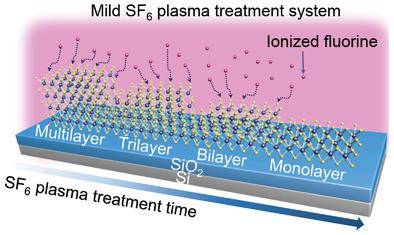
Low‐Damaged Layer‐by‐Layer Etching of Large‐Area Molybdenum Disulfide Films via Mild Plasma Treatment
Advanced Materials Interfaces ( IF 5.4 ) Pub Date : 2020-07-21 , DOI: 10.1002/admi.202000762 Sang‐Soo Chee 1 , Moon‐Ho Ham 1
Advanced Materials Interfaces ( IF 5.4 ) Pub Date : 2020-07-21 , DOI: 10.1002/admi.202000762 Sang‐Soo Chee 1 , Moon‐Ho Ham 1
Affiliation
|
Controlling the number of layers of 2D transition metal dichalcogenide (TMDC) film is indispensable for optoelectronic applications because of their layer‐dependent optical features. However, most of methodologies on controlling TMDC layers induce undesirable defect formation and are performed on TMDC flakes, obtained from mechanical exfoliation. These limitations make practical TMDC‐based optoelectronic applications more difficult. Herein, layer‐by‐layer etching methodology of molybdenum disulfide (MoS2) films is developed using mild sulfur hexafluoride (SF6) plasma treatment. It is confirmed that the number of layers is successfully controlled from trilayer to monolayer by increasing plasma treatment time, while preserving overall film quality. Such low‐damaged layer‐by‐layer etching is attributed to this mild plasma etching system to only introduce the chemical reaction between ionized fluorine and MoS2, without physical damage to MoS2. Electrical properties of layer‐controlled MoS2 devices are also investigated, achieving comparatively high field‐effect mobilities of 16.2, 8.84, and 2.87 cm2 V−1 s−1 for tri‐, bi‐, and monolayer MoS2, respectively. This finding provides the possibility of realizing layer‐by‐layer engineering of 2D TMDCs.
中文翻译:

通过轻度等离子体处理对大面积二硫化钼薄膜进行低损伤的逐层蚀刻
由于2D过渡金属二硫化碳(TMDC)膜的层依赖性光学特性,因此控制光电层中的膜层数是必不可少的。但是,大多数控制TMDC层的方法会导致不良的缺陷形成,并且会对通过机械剥落获得的TMDC薄片进行处理。这些限制使基于TMDC的实际光电应用更加困难。在此,使用轻度六氟化硫(SF 6)开发了二硫化钼(MoS 2)膜的逐层蚀刻方法)等离子处理。证实了通过增加等离子体处理时间成功地控制了从三层到单层的层数,同时保留了总体膜质量。这种低损坏的逐层蚀刻归因于这种温和的等离子体蚀刻系统,该系统仅引入了离子化的氟与MoS 2之间的化学反应,而没有对MoS 2造成物理损坏。还研究了层控制的MoS 2器件的电性能,对于三层,双层和单层MoS 2,实现了16.2、8.84和2.87 cm 2 V -1 s -1的较高场效应迁移率, 分别。这一发现为实现二维TMDC的逐层工程提供了可能性。
更新日期:2020-09-11
中文翻译:
通过轻度等离子体处理对大面积二硫化钼薄膜进行低损伤的逐层蚀刻
由于2D过渡金属二硫化碳(TMDC)膜的层依赖性光学特性,因此控制光电层中的膜层数是必不可少的。但是,大多数控制TMDC层的方法会导致不良的缺陷形成,并且会对通过机械剥落获得的TMDC薄片进行处理。这些限制使基于TMDC的实际光电应用更加困难。在此,使用轻度六氟化硫(SF 6)开发了二硫化钼(MoS 2)膜的逐层蚀刻方法)等离子处理。证实了通过增加等离子体处理时间成功地控制了从三层到单层的层数,同时保留了总体膜质量。这种低损坏的逐层蚀刻归因于这种温和的等离子体蚀刻系统,该系统仅引入了离子化的氟与MoS 2之间的化学反应,而没有对MoS 2造成物理损坏。还研究了层控制的MoS 2器件的电性能,对于三层,双层和单层MoS 2,实现了16.2、8.84和2.87 cm 2 V -1 s -1的较高场效应迁移率, 分别。这一发现为实现二维TMDC的逐层工程提供了可能性。


 京公网安备 11010802027423号