当前位置:
X-MOL 学术
›
Phys. Status Solidi. Rapid Res. Lett.
›
论文详情
Our official English website, www.x-mol.net, welcomes your feedback! (Note: you will need to create a separate account there.)
Dielectric/Semiconductor Interfacial p‐Doping: A New Technique to Fabricate Solution‐Processed High‐Performance 1 V Ambipolar Oxide Transistors
Physica Status Solidi-Rapid Research Letters ( IF 2.8 ) Pub Date : 2020-07-21 , DOI: 10.1002/pssr.202000268 Nitesh K. Chourasia, Anand Sharma, Nila Pal, Sajal Biring, Bhola N. Pal
Physica Status Solidi-Rapid Research Letters ( IF 2.8 ) Pub Date : 2020-07-21 , DOI: 10.1002/pssr.202000268 Nitesh K. Chourasia, Anand Sharma, Nila Pal, Sajal Biring, Bhola N. Pal
|
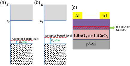
Herein, dielectric/semiconductor interfacial p‐doping is used to develop a high‐carrier‐mobility and balanced ambipolar tin oxide (SnO2) thin‐film transistor (TFT). To introduce this interfacial doping, TFTs are fabricated by using two different ion‐conducting oxide dielectrics containing trivalent atoms. These ion‐conducting dielectrics are LiInO2 and LiGaO2 containing a mobile Li+ ion that reduces the operating voltage of these TFTs to ≤2.0 V. During SnO2 thin film deposition, the interfacial SnO2 layer is p‐doped by an In or Ga atom of the gate dielectric and therefore, hole conduction is facilitated in the channel of the TFT. To realize this interfacial doping phenomenon, a reference TFT is fabricated with a Li2ZnO2 dielectric that contains a divalent zinc atom. Comparative electrical data indicate that TFTs with LiInO2 and LiGaO2 dielectrics are ambipolar in nature, whereas the TFT with a Li2ZnO2 dielectric is a unipolar n‐channel transistor, corroborating the interfacial doping of SnO2. Most interestingly, using a LiInO2 dielectric, a 1.0 V balanced ambipolar TFT with high electron and hole mobility values of 7 and 8 cm2 V−1 s−1, respectively, can be fabricated, with an on/off ratio > 102 for both operations. The TFT with a LiInO2 dielectric is utilized successfully to fabricate a low‐voltage complementary metal–oxide–semiconductor (CMOS) inverter.
中文翻译:

介电/半导体界面p掺杂:制造溶液处理的高性能1 V双极性氧化晶体管的新技术
本文中,电介质/半导体界面p掺杂用于开发高载流子迁移率和平衡的双极性氧化锡(SnO 2)薄膜晶体管(TFT)。为了引入这种界面掺杂,通过使用两种包含三价原子的不同离子导电氧化物电介质来制造TFT。这些离子传导性电介质为LiInO 2和LiGaO 2,其中含有可移动的Li +离子,可将这些TFT的工作电压降至≤2.0V。在SnO 2薄膜沉积过程中,界面SnO 2栅极电介质的In或Ga原子p掺杂了Pb层,因此,在TFT的沟道中促进了空穴传导。为了实现这种界面掺杂现象,利用包含二价锌原子的Li 2 ZnO 2电介质来制造参考TFT 。比较电数据表明,具有LiInO 2和LiGaO 2介电质的TFT本质上是双极性的,而具有Li 2 ZnO 2介电质的TFT是单极n沟道晶体管,这证实了SnO 2的界面掺杂。最有趣的是,使用LiInO 2电介质,1.0 V平衡双极性TFT,其电子和空穴迁移率值分别为7和8 cm可以分别制造2 V -1 s -1,两种操作的开/关比> 10 2。具有LiInO 2电介质的TFT已成功用于制造低压互补金属氧化物半导体(CMOS)逆变器。
更新日期:2020-07-21
中文翻译:
介电/半导体界面p掺杂:制造溶液处理的高性能1 V双极性氧化晶体管的新技术
本文中,电介质/半导体界面p掺杂用于开发高载流子迁移率和平衡的双极性氧化锡(SnO 2)薄膜晶体管(TFT)。为了引入这种界面掺杂,通过使用两种包含三价原子的不同离子导电氧化物电介质来制造TFT。这些离子传导性电介质为LiInO 2和LiGaO 2,其中含有可移动的Li +离子,可将这些TFT的工作电压降至≤2.0V。在SnO 2薄膜沉积过程中,界面SnO 2栅极电介质的In或Ga原子p掺杂了Pb层,因此,在TFT的沟道中促进了空穴传导。为了实现这种界面掺杂现象,利用包含二价锌原子的Li 2 ZnO 2电介质来制造参考TFT 。比较电数据表明,具有LiInO 2和LiGaO 2介电质的TFT本质上是双极性的,而具有Li 2 ZnO 2介电质的TFT是单极n沟道晶体管,这证实了SnO 2的界面掺杂。最有趣的是,使用LiInO 2电介质,1.0 V平衡双极性TFT,其电子和空穴迁移率值分别为7和8 cm可以分别制造2 V -1 s -1,两种操作的开/关比> 10 2。具有LiInO 2电介质的TFT已成功用于制造低压互补金属氧化物半导体(CMOS)逆变器。


 京公网安备 11010802027423号