当前位置:
X-MOL 学术
›
ACS Appl. Electron. Mater.
›
论文详情
Our official English website, www.x-mol.net, welcomes your feedback! (Note: you will need to create a separate account there.)
Engineering Architecture of Quantum Dot-Based Light-Emitting Diode for High Device Performance with Double-Sided Emission Fabricated by Nonvacuum Technique
ACS Applied Electronic Materials ( IF 4.7 ) Pub Date : 2020-07-08 , DOI: 10.1021/acsaelm.0c00332 Sajid Hussain 1 , Alagesan Subramanian 1 , Shikai Yan 1 , Nasrud Din 1 , Ghulam Abbas 2 , Ahmed Shuja 3 , Wei Lei 1 , Qasim Khan 1, 2, 4
ACS Applied Electronic Materials ( IF 4.7 ) Pub Date : 2020-07-08 , DOI: 10.1021/acsaelm.0c00332 Sajid Hussain 1 , Alagesan Subramanian 1 , Shikai Yan 1 , Nasrud Din 1 , Ghulam Abbas 2 , Ahmed Shuja 3 , Wei Lei 1 , Qasim Khan 1, 2, 4
Affiliation
|
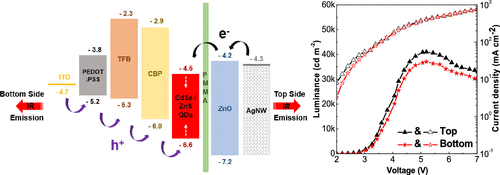
The CdSe/ZnS quantum dots (QDs) have drawn the attention of the researchers due to their superior photophysical properties and their applications in QD-based light-emitting diodes (QLEDs). The conventional CdSe/ZnS-based QLED uses a highly conductive electron-transport layer, low-mobility hole-transporting layers (HTLs), and a vacuum-deposited opaque metal electrode at the top. This structure renders unbalanced charge injection into the emissive layer and also allows the device to emit light only at the bottom side, which affects the device output luminance and stability. Moreover, in the vacuum-deposition technique, the fabrication process is more complex, expensive, and time-consuming. To address all these issues, we fabricated an all-solution processable double-sided emitting QLED by a nonvacuum technique using high mobility multi-HTLs with a cascade structure, an insulating layer, and a transparent silver nanowire (AgNW) electrode for balanced charge injection for obtaining higher luminance at the top-side AgNW electrode. The as-fabricated QLED exhibited a very low turn-on voltage and high luminance of 2.2 V and 41,010 cd m–2, respectively. The QLED has also shown a high current efficiency of 15.2 cd A–1, a luminous efficiency of 16.2 lm W–1, and an external quantum efficiency of 8.2% at the top-side. These results indicate that the double-sided emitting QLED device opens up a pathway for designing next-generation lighting and display devices.
中文翻译:

非真空技术制造的双面发光双量子点发光二极管的工程架构
CdSe / ZnS量子点(QDs)由于其出色的光物理特性及其在基于QD的发光二极管(QLED)中的应用而吸引了研究人员的注意。常规的基于CdSe / ZnS的QLED在顶部使用高导电性电子传输层,低迁移率空穴传输层(HTL)和真空沉积的不透明金属电极。这种结构使不平衡的电荷注入到发射层中,并且还使器件仅在底侧发光,这会影响器件的输出亮度和稳定性。此外,在真空沉积技术中,制造过程更复杂,昂贵且耗时。为了解决所有这些问题,我们通过非真空技术,使用具有级联结构的高迁移率多HTL,绝缘层和透明银纳米线(AgNW)电极,通过平衡电荷注入,获得了全溶液可处理的双面发光QLED,从而获得了更高的亮度顶部AgNW电极。制成的QLED表现出非常低的开启电压和2.2 V和41,010 cd m的高亮度–2分别。QLED还显示出15.2 cd A –1的高电流效率,16.2 lm W –1的发光效率以及顶部的8.2%的外部量子效率。这些结果表明,双面发射QLED器件为设计下一代照明和显示设备开辟了道路。
更新日期:2020-08-25
中文翻译:
非真空技术制造的双面发光双量子点发光二极管的工程架构
CdSe / ZnS量子点(QDs)由于其出色的光物理特性及其在基于QD的发光二极管(QLED)中的应用而吸引了研究人员的注意。常规的基于CdSe / ZnS的QLED在顶部使用高导电性电子传输层,低迁移率空穴传输层(HTL)和真空沉积的不透明金属电极。这种结构使不平衡的电荷注入到发射层中,并且还使器件仅在底侧发光,这会影响器件的输出亮度和稳定性。此外,在真空沉积技术中,制造过程更复杂,昂贵且耗时。为了解决所有这些问题,我们通过非真空技术,使用具有级联结构的高迁移率多HTL,绝缘层和透明银纳米线(AgNW)电极,通过平衡电荷注入,获得了全溶液可处理的双面发光QLED,从而获得了更高的亮度顶部AgNW电极。制成的QLED表现出非常低的开启电压和2.2 V和41,010 cd m的高亮度–2分别。QLED还显示出15.2 cd A –1的高电流效率,16.2 lm W –1的发光效率以及顶部的8.2%的外部量子效率。这些结果表明,双面发射QLED器件为设计下一代照明和显示设备开辟了道路。


 京公网安备 11010802027423号