当前位置:
X-MOL 学术
›
Phys. Status Solidi. Rapid Res. Lett.
›
论文详情
Our official English website, www.x-mol.net, welcomes your feedback! (Note: you will need to create a separate account there.)
Tuning the Conductivity Type in Monolayer WS2 and MoS2 by Sulfur Vacancies
Physica Status Solidi-Rapid Research Letters ( IF 2.8 ) Pub Date : 2020-07-02 , DOI: 10.1002/pssr.202000248 Jing Yang 1 , Fabio Bussolotti 2 , Hiroyo Kawai 1 , Kuan Eng Johnson Goh 2, 3
Physica Status Solidi-Rapid Research Letters ( IF 2.8 ) Pub Date : 2020-07-02 , DOI: 10.1002/pssr.202000248 Jing Yang 1 , Fabio Bussolotti 2 , Hiroyo Kawai 1 , Kuan Eng Johnson Goh 2, 3
Affiliation
|
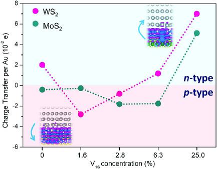
While n‐type behavior appears to be more common in as‐prepared two‐dimensional (2D) transition metal dichalcogenides (TMDCs), substitutional doping with electron accepting atoms is typically required to tune the conductivity to p‐type in order to facilitate their potential application in different devices. Herein, a systematic study is reported on the equivalent electrical “doping” effect of single sulfur vacancies (V1S) in monolayer WS2 and MoS2 by studying the interface interaction of WS2–Au and MoS2–Au contacts. Based on the first principles calculations, it is found that the V1S can significantly alter the semiconductor behavior of both monolayer WS2 and MoS2 so that they can exhibit the character of electron acceptor (p‐type) as well as electron donor (n‐type) when they are contacted with gold. For relatively low V1S densities (approximately <7% for MoS2 and <3% for WS2), the monolayer TMDC serves as electron acceptor. As the V1S density increases beyond the threshold densities, the MoS2 and WS2 play the role of electron donor. The significant impact V1S can have on monolayer WS2 and MoS2 may be useful for engineering its electrical behavior and offers an alternative way to tune the semiconductor TMDCs to exhibit either n‐type or p‐type behavior.
中文翻译:

通过硫空位调整WS2和MoS2单层中的电导类型
尽管在制备的二维(2D)过渡金属二硫化二碳(TMDC)中n型行为似乎更常见,但通常需要用电子接受原子进行取代掺杂以将电导率调整为p型,以促进其势能在不同设备上的应用程序。本文中,通过研究WS 2 –Au和MoS 2 –Au接触的界面相互作用,对单层WS 2和MoS 2中单硫空位(V 1S)的等效电“掺杂”效应进行了系统研究。根据第一个原理计算,发现V 1S可以显着改变单层WS 2和MoS 2的半导体性能,因此当它们与金接触时,它们可以表现出电子受体(p型)和电子给体(n型)的特性。对于相对较低的V 1S密度(MoS 2约为<7%,WS 2约为< 3%),单层TMDC用作电子受体。当V 1S密度增加到超过阈值密度时,MoS 2和WS 2发挥电子给体的作用。V 1S可能对单层WS 2和MoS 2产生重大影响可能对于工程化其电学行为很有用,并提供了一种替代方法来调节半导体TMDC以表现出n型或p型行为。
更新日期:2020-09-08
中文翻译:
通过硫空位调整WS2和MoS2单层中的电导类型
尽管在制备的二维(2D)过渡金属二硫化二碳(TMDC)中n型行为似乎更常见,但通常需要用电子接受原子进行取代掺杂以将电导率调整为p型,以促进其势能在不同设备上的应用程序。本文中,通过研究WS 2 –Au和MoS 2 –Au接触的界面相互作用,对单层WS 2和MoS 2中单硫空位(V 1S)的等效电“掺杂”效应进行了系统研究。根据第一个原理计算,发现V 1S可以显着改变单层WS 2和MoS 2的半导体性能,因此当它们与金接触时,它们可以表现出电子受体(p型)和电子给体(n型)的特性。对于相对较低的V 1S密度(MoS 2约为<7%,WS 2约为< 3%),单层TMDC用作电子受体。当V 1S密度增加到超过阈值密度时,MoS 2和WS 2发挥电子给体的作用。V 1S可能对单层WS 2和MoS 2产生重大影响可能对于工程化其电学行为很有用,并提供了一种替代方法来调节半导体TMDC以表现出n型或p型行为。


 京公网安备 11010802027423号