当前位置:
X-MOL 学术
›
Adv. Mater. Technol.
›
论文详情
Our official English website, www.x-mol.net, welcomes your feedback! (Note: you will need to create a separate account there.)
High Resolution Soft and Stretchable Circuits with PVA/Liquid‐Metal Mediated Printing
Advanced Materials Technologies ( IF 6.8 ) Pub Date : 2020-06-30 , DOI: 10.1002/admt.202000343 André F. Silva 1 , Hugo Paisana 1 , Tânia Fernandes 2 , Joana Góis 2 , Arménio Serra 2 , Jorge F. J. Coelho 2 , Aníbal T. Almeida 1 , Carmel Majidi 3 , Mahmoud Tavakoli 1
Advanced Materials Technologies ( IF 6.8 ) Pub Date : 2020-06-30 , DOI: 10.1002/admt.202000343 André F. Silva 1 , Hugo Paisana 1 , Tânia Fernandes 2 , Joana Góis 2 , Arménio Serra 2 , Jorge F. J. Coelho 2 , Aníbal T. Almeida 1 , Carmel Majidi 3 , Mahmoud Tavakoli 1
Affiliation
|
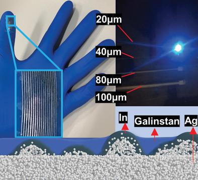
A novel technique that permits, for the first time, fabrication of stretchable traces with linewidths as low as 20 µm and line‐spacing of 30 µm, based on simple coating and printing techniques, performed entirely at ambient condition, is demonstrated. By relying on existing inkjet printing technique, the proposed sinter‐free method is a step toward scalable fabrication of high‐resolution stretchable circuits, with application in logic gates, transparent conductors, and solar panels. This is accomplished by coating a layer of poly(vinyl alcohol) (PVA) over an elastic substrate, inkjet printing a circuit with silver nanoparticle (AgNP) ink, and then coating the printed circuit with a thin film of eutectic gallium‐indium‐tin (Galinstan) alloy. The Galinstan coating selectively wets to the printed AgNPs, resulting in highly conductive (6.65 × 10⁶ S m−1) circuits that can withstand over 100% of strain with a modest gauge factor of ≈2.7. The process does not need thermal sintering, thanks to the Galinstan fusion with AgNPs, thus being compatible with heat‐sensitive substrates. The PVA coating has a critical role as a hydrophilic surface that absorbs the water‐based ink but resists wetting of the Galinstan. This method is demonstrated over a variety of substrates, including ultrasoft polyurethanes, ultra‐stretchable styrene–ethylene/butylynestyrene, and polyimide.
中文翻译:

具有PVA /液态金属介导印刷的高分辨率软性和可拉伸电路
展示了一种新颖的技术,该技术首次通过简单的涂布和印刷技术首次在完全的环境条件下进行生产,线宽低至20 µm,线间距为30 µm。通过依靠现有的喷墨打印技术,所提出的无烧结方法是朝着可伸缩制造高分辨率可拉伸电路的方向迈出的一步,并将其应用于逻辑门,透明导体和太阳能电池板。这是通过在弹性基材上涂覆一层聚乙烯醇(PVA),用银纳米颗粒(AgNP)油墨喷墨印刷电路,然后在印刷电路上涂覆共晶镓铟锡薄膜来实现的(加林斯坦)合金。Galinstan涂层有选择地润湿印刷的AgNP,从而获得高导电性(6.65×10⁶ S m -1)电路可以承受100%以上的应变,且应变系数为≈2.7。由于Galinstan与AgNP融合,因此该工艺不需要热烧结,因此与热敏基材兼容。PVA涂层作为亲水性表面起着至关重要的作用,它可以吸收水性墨水,但可以防止加仑斯坦的润湿。该方法已在多种基材上得到证明,包括超软聚氨酯,超可拉伸的苯乙烯-乙烯/丁炔苯乙烯和聚酰亚胺。
更新日期:2020-06-30
中文翻译:
具有PVA /液态金属介导印刷的高分辨率软性和可拉伸电路
展示了一种新颖的技术,该技术首次通过简单的涂布和印刷技术首次在完全的环境条件下进行生产,线宽低至20 µm,线间距为30 µm。通过依靠现有的喷墨打印技术,所提出的无烧结方法是朝着可伸缩制造高分辨率可拉伸电路的方向迈出的一步,并将其应用于逻辑门,透明导体和太阳能电池板。这是通过在弹性基材上涂覆一层聚乙烯醇(PVA),用银纳米颗粒(AgNP)油墨喷墨印刷电路,然后在印刷电路上涂覆共晶镓铟锡薄膜来实现的(加林斯坦)合金。Galinstan涂层有选择地润湿印刷的AgNP,从而获得高导电性(6.65×10⁶ S m -1)电路可以承受100%以上的应变,且应变系数为≈2.7。由于Galinstan与AgNP融合,因此该工艺不需要热烧结,因此与热敏基材兼容。PVA涂层作为亲水性表面起着至关重要的作用,它可以吸收水性墨水,但可以防止加仑斯坦的润湿。该方法已在多种基材上得到证明,包括超软聚氨酯,超可拉伸的苯乙烯-乙烯/丁炔苯乙烯和聚酰亚胺。


 京公网安备 11010802027423号