Applied Materials Today ( IF 8.3 ) Pub Date : 2020-06-30 , DOI: 10.1016/j.apmt.2020.100734 Pranab K Mohapatra , Kamalakannan Ranganathan , Lital Dezanashvili , Lothar Houben , Ariel Ismach
|
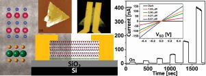
One of the most intriguing properties of layered materials is their ability to form inherently ultra-thin atomically sharp vertical interfaces and hybrid layered compounds, in moderate environment conditions, which are ideal platforms for both, scientific research and many applications. Here, we present the selective van der Waals epitaxial formation of β-In2Se3 on transition metal dichalcogenides (TMDCs). This is achieved in a two-step chemical vapor deposition (CVD) process, in which first, the monolayer TMDC, is synthesized and then the β-In2Se3 is grown on top of it. The thickness of the second phase can be controlled by the growth conditions, while the crystal size is dictated by the MoS2 single-crystal domain size. High-resolution transmission electron microscope (HRTEM) studies reveal a clean and sharp interface, while selected area diffraction (SAED) demonstrates a clear registry between both phases. The hybrid layered-compound exhibit better electrical transport than the intrinsic indium-selenide layer. The high crystallinity of In2Se3 grown on MoS2 yield fast response among the CVD-derived In2Se3-based photodetectors with rise/fall times of 4/7 ms, photoresponsivity of up to ~23 A/W and specific detectivity of ~ 5 × 10¹¹. Our methodology allows high quality thin In2Se3 layers to be formed via van der Waals epitaxy on TMDCs, forming complex vertical heterostructures for optoelectronic applications.
中文翻译:
高性能光电探测器在单层过渡金属二卤化二单晶上In 2 Se 3的外延生长
层状材料最令人着迷的特性之一是它们能够在中等环境条件下形成固有的超薄原子锐利的垂直界面和杂化层状化合物的能力,这是科学研究和许多应用的理想平台。这里,我们提出范德华外延形成的选择性面包车β -In 2硒3上的过渡金属二硫属化物(TMDCs)。这是通过两步化学气相沉积(CVD)工艺实现的,其中首先合成单层TMDC,然后合成β- In 2 Se 3在它之上生长。第二相的厚度可以由生长条件控制,而晶体尺寸由MoS 2单晶畴尺寸决定。高分辨率透射电子显微镜(HRTEM)的研究揭示了干净而锐利的界面,而选定区域衍射(SAED)则显示了两个相之间的清晰配准。杂化层状化合物表现出比本征硒化铟层更好的电传输。MoS 2上生长的In 2 Se 3的高结晶度在CVD衍生的In 2 Se 3中产生快速响应的光电探测器,其上升/下降时间为4/7 ms,光响应度高达〜23 A / W,比灵敏度为〜5×10 11。我们的方法允许通过TMDC上的范德华外延形成高质量的In 2 Se 3薄层,从而形成用于光电应用的复杂垂直异质结构。


 京公网安备 11010802027423号