当前位置:
X-MOL 学术
›
Appl. Surf. Sci.
›
论文详情
Our official English website, www.x-mol.net, welcomes your feedback! (Note: you will need to create a separate account there.)
Wafer-scale fabrication of single-crystal graphene on Ge(110) substrate by optimized CH4/H2 ratio
Applied Surface Science ( IF 6.7 ) Pub Date : 2020-11-01 , DOI: 10.1016/j.apsusc.2020.147066 Tianbo Wang , Panlin Li , Xudong Hu , Min Gao , Zengfeng Di , Zhongying Xue , Miao Zhang
Applied Surface Science ( IF 6.7 ) Pub Date : 2020-11-01 , DOI: 10.1016/j.apsusc.2020.147066 Tianbo Wang , Panlin Li , Xudong Hu , Min Gao , Zengfeng Di , Zhongying Xue , Miao Zhang
|
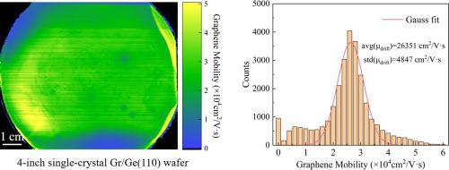
Abstract The synthesis of high-quality wafer-scale single-crystal graphene is indispensable for the commercial applications of graphene-based electronic and photonic devices. Previously large-scale single-crystal graphene was successfully acquired by various growth optimization whereas the methods vary from lab to lab due to the complicated process of chemical vapor deposition. Here we present an approach to fabricate monolayer single-crystal graphene on 4-inch Ge(1 1 0) wafer by tuning CH4/H2 ratio precisely. By directly monitoring the growth process of graphene via atomic force microscopy, it is found that under high CH4/H2 ratio condition new graphene domains ceaselessly nucleate and enlarge during the whole growth process, while under low CH4/H2 ratio condition, the density of graphene domains is saturated at early stage, which causes the formation of single-crystal graphene. Terahertz time domain spectroscopy shows that the average carrier mobility of single-crystal graphene wafer is as high as 26351 cm2/V·s, comparable to that of the exfoliated graphene. This work provides an efficient and reliable approach to fabricate wafer-scale single-crystal graphene for microelectronics and optoelectronics applications in the future.
中文翻译:

通过优化的 CH4/H2 比在 Ge(110) 衬底上晶圆级制造单晶石墨烯
摘要 高质量晶圆级单晶石墨烯的合成对于基于石墨烯的电子和光子器件的商业应用是必不可少的。以前通过各种生长优化成功获得了大规模单晶石墨烯,但由于化学气相沉积的复杂过程,方法因实验室而异。在这里,我们提出了一种通过精确调整 CH4/H2 比率在 4 英寸 Ge(1 1 0) 晶片上制造单层单晶石墨烯的方法。通过原子力显微镜直接监测石墨烯的生长过程,发现在高 CH4/H2 比条件下,新的石墨烯畴在整个生长过程中不断成核和扩大,而在低 CH4/H2 比条件下,石墨烯的密度域在早期就饱和了,这导致单晶石墨烯的形成。太赫兹时域光谱表明,单晶石墨烯晶片的平均载流子迁移率高达26351 cm2/V·s,与剥离石墨烯相当。这项工作为未来制造用于微电子和光电子应用的晶圆级单晶石墨烯提供了一种有效且可靠的方法。
更新日期:2020-11-01
中文翻译:
通过优化的 CH4/H2 比在 Ge(110) 衬底上晶圆级制造单晶石墨烯
摘要 高质量晶圆级单晶石墨烯的合成对于基于石墨烯的电子和光子器件的商业应用是必不可少的。以前通过各种生长优化成功获得了大规模单晶石墨烯,但由于化学气相沉积的复杂过程,方法因实验室而异。在这里,我们提出了一种通过精确调整 CH4/H2 比率在 4 英寸 Ge(1 1 0) 晶片上制造单层单晶石墨烯的方法。通过原子力显微镜直接监测石墨烯的生长过程,发现在高 CH4/H2 比条件下,新的石墨烯畴在整个生长过程中不断成核和扩大,而在低 CH4/H2 比条件下,石墨烯的密度域在早期就饱和了,这导致单晶石墨烯的形成。太赫兹时域光谱表明,单晶石墨烯晶片的平均载流子迁移率高达26351 cm2/V·s,与剥离石墨烯相当。这项工作为未来制造用于微电子和光电子应用的晶圆级单晶石墨烯提供了一种有效且可靠的方法。


 京公网安备 11010802027423号