Nano Energy ( IF 17.6 ) Pub Date : 2020-06-28 , DOI: 10.1016/j.nanoen.2020.105072 R. Khoury , J. Alvarez , T. Ohashi , I. Martín , P. Ortega , G. López , C. Jin , Z. Li , Rusli , P. Bulkin , E.V. Johnson
|
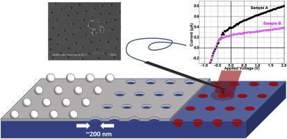
Localized p-doped nanojunctions (200–300 nm in diameter) were formed in n-type crystalline silicon substrates and were characterized using scanning electron microscopy (SEM) and conductive-probe atomic force microscopy (C-AFM). Localized doping was performed by diffusion through sub-micron sized holes in a silicon-oxide mask defined using self-organized polystyrene nanoparticles. After oxide removal, a significant brightness contrast in the SEM top and side view images strongly suggested the successful local doping of these areas. Furthermore, local current-voltage measurements performed by C-AFM revealed an open circuit voltage and a short-circuit current only in the areas defined as nanojunctions. This photovoltaic effect is driven by the laser used to control cantilever deflection in the AFM.
中文翻译:
使用导电探针AFM观察局部掺杂的硅纳米结内的光伏效应
在n型晶体硅衬底中形成局部掺杂的p型掺杂纳米结(直径200-300 nm),并使用扫描电子显微镜(SEM)和导电探针原子力显微镜(C-AFM)对其进行表征。通过扩散通过使用自组织聚苯乙烯纳米粒子定义的氧化硅掩模中的亚微米大小的孔来进行局部掺杂。去除氧化物后,SEM顶视图和侧视图图像中明显的亮度对比强烈暗示了这些区域的成功局部掺杂。此外,由C-AFM执行的局部电流-电压测量仅在定义为纳米结的区域显示出开路电压和短路电流。这种光电效应是由用于控制AFM中悬臂偏转的激光驱动的。


 京公网安备 11010802027423号