Our official English website, www.x-mol.net, welcomes your feedback! (Note: you will need to create a separate account there.)
Layer-Selective Synthesis of MoS2 and WS2 Structures under Ambient Conditions for Customized Electronics.
ACS Nano ( IF 17.1 ) Pub Date : 2020-06-24 , DOI: 10.1021/acsnano.0c02745 Seoungwoong Park 1, 2 , Aram Lee 1 , Kwang-Hun Choi 1 , Seok-Ki Hyeong 1 , Sukang Bae 1 , Jae-Min Hong 1 , Tae-Wook Kim 3 , Byung Hee Hong 2 , Seoung-Ki Lee 1
ACS Nano ( IF 17.1 ) Pub Date : 2020-06-24 , DOI: 10.1021/acsnano.0c02745 Seoungwoong Park 1, 2 , Aram Lee 1 , Kwang-Hun Choi 1 , Seok-Ki Hyeong 1 , Sukang Bae 1 , Jae-Min Hong 1 , Tae-Wook Kim 3 , Byung Hee Hong 2 , Seoung-Ki Lee 1
Affiliation
|
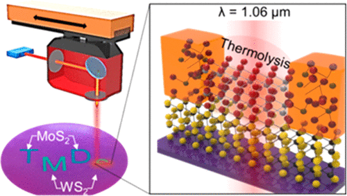
Transition metal dichalcogenides (TMDs) have attracted significant interest as one of the key materials in future electronics such as logic devices, optoelectrical devices, and wearable electronics. However, a complicated synthesis method and multistep processes for device fabrication pose major hurdles for their practical applications. Here, we introduce a direct and rapid method for layer-selective synthesis of MoS2 and WS2 structures in wafer-scale using a pulsed laser annealing system (λ = 1.06 μm, pulse duration ∼100 ps) in ambient conditions. The precursor layer of each TMD, which has at least 3 orders of magnitude higher absorption coefficient than those of neighboring layers, rigorously absorbed the incoming energy of the laser pulse and rapidly pyrolyzed in a few nanoseconds, enabling the generation of a MoS2 or WS2 layer without damaging the adjacent layers of SiO2 or polymer substrate. Through experimental and theoretical studies, we establish the underlying principles of selective synthesis and optimize the laser annealing conditions, such as laser wavelength, output power, and scribing speed, under ambient condition. As a result, individual homostructures of patterned MoS2 and WS2 layers were directly synthesized on a 4 in. wafer. Moreover, a consecutive synthesis of the second layer on top of the first synthesized layer realized a vertically stacked WS2/MoS2 heterojunction structure, which can be treated as a cornerstone of electronic devices. As a proof of concept, we demonstrated the behavior of a MoS2-based field-effect transistor, a skin-attachable motion sensor, and a MoS2/WS2-based heterojunction diode in this study. The ultrafast and selective synthesis of the TMDs suggests an approach to the large-area/mass production of functional heterostructure-based electronics.
中文翻译:

定制电子环境条件下MoS2和WS2结构的层选择性合成。
作为未来电子产品(例如逻辑器件,光电器件和可穿戴电子产品)中的关键材料之一,过渡金属二硫化碳(TMD)引起了人们的极大兴趣。然而,用于器件制造的复杂的合成方法和多步工艺对其实际应用构成了主要障碍。在这里,我们介绍一种直接快速的方法,用于MoS 2和WS 2的层选择性合成在环境条件下使用脉冲激光退火系统(λ= 1.06μm,脉冲持续时间〜100 ps)在晶片规模上构造结构。每个TMD的前体层比相邻层的吸收系数至少高3个数量级,它严格吸收激光脉冲的入射能量并在几纳秒内迅速热解,从而生成MoS 2或WS 2层而不会损坏相邻的SiO 2层或聚合物基材。通过实验和理论研究,我们建立了选择性合成的基本原理,并在环境条件下优化了激光退火条件,例如激光波长,输出功率和刻划速度。结果,图案化的MoS 2和WS 2层的各个同质结构直接在4英寸晶圆上合成。而且,在第一合成层的顶部上对第二层的连续合成实现了垂直堆叠的WS 2 / MoS 2异质结结构,可以将其视为电子设备的基石。作为概念的证明,我们演示了MoS 2的行为这项研究中,基于半导体的场效应晶体管,皮肤可附着的运动传感器和基于MoS 2 / WS 2的异质结二极管。TMD的超快速和选择性合成表明了一种大面积/批量生产基于功能异质结构的电子产品的方法。
更新日期:2020-07-28
中文翻译:
定制电子环境条件下MoS2和WS2结构的层选择性合成。
作为未来电子产品(例如逻辑器件,光电器件和可穿戴电子产品)中的关键材料之一,过渡金属二硫化碳(TMD)引起了人们的极大兴趣。然而,用于器件制造的复杂的合成方法和多步工艺对其实际应用构成了主要障碍。在这里,我们介绍一种直接快速的方法,用于MoS 2和WS 2的层选择性合成在环境条件下使用脉冲激光退火系统(λ= 1.06μm,脉冲持续时间〜100 ps)在晶片规模上构造结构。每个TMD的前体层比相邻层的吸收系数至少高3个数量级,它严格吸收激光脉冲的入射能量并在几纳秒内迅速热解,从而生成MoS 2或WS 2层而不会损坏相邻的SiO 2层或聚合物基材。通过实验和理论研究,我们建立了选择性合成的基本原理,并在环境条件下优化了激光退火条件,例如激光波长,输出功率和刻划速度。结果,图案化的MoS 2和WS 2层的各个同质结构直接在4英寸晶圆上合成。而且,在第一合成层的顶部上对第二层的连续合成实现了垂直堆叠的WS 2 / MoS 2异质结结构,可以将其视为电子设备的基石。作为概念的证明,我们演示了MoS 2的行为这项研究中,基于半导体的场效应晶体管,皮肤可附着的运动传感器和基于MoS 2 / WS 2的异质结二极管。TMD的超快速和选择性合成表明了一种大面积/批量生产基于功能异质结构的电子产品的方法。


 京公网安备 11010802027423号