当前位置:
X-MOL 学术
›
Adv. Funct. Mater.
›
论文详情
Our official English website, www.x-mol.net, welcomes your feedback! (Note: you will need to create a separate account there.)
Process Pathway Controlled Evolution of Phase and Van‐der‐Waals Epitaxy in In/In2O3 on Graphene Heterostructures
Advanced Functional Materials ( IF 19.0 ) Pub Date : 2020-06-24 , DOI: 10.1002/adfm.202003300 Kenan Elibol 1 , Clemens Mangler 1 , Tushar Gupta 2 , Georg Zagler 1 , Dominik Eder 2 , Jannik C. Meyer 1 , Jani Kotakoski 1 , Bernhard C. Bayer 1, 2
Advanced Functional Materials ( IF 19.0 ) Pub Date : 2020-06-24 , DOI: 10.1002/adfm.202003300 Kenan Elibol 1 , Clemens Mangler 1 , Tushar Gupta 2 , Georg Zagler 1 , Dominik Eder 2 , Jannik C. Meyer 1 , Jani Kotakoski 1 , Bernhard C. Bayer 1, 2
Affiliation
|
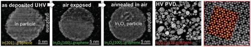
Many applications of 2D materials require deposition of non‐2D metals and metal‐oxides onto the 2D materials. Little is however known about the mechanisms of such non‐2D/2D interfacing, particularly at the atomic scale. Here, atomically resolved scanning transmission electron microscopy (STEM) is used to follow the entire physical vapor deposition (PVD) cycle of application‐relevant non‐2D In/In2O3 nanostructures on graphene. First, a “quasi‐in‐situ” approach with indium being in situ evaporated onto graphene in oxygen‐/water‐free ultra‐high‐vacuum (UHV) is employed, followed by STEM imaging without vacuum break and then repeated controlled ambient air exposures and reloading into STEM. This allows stepwise monitoring of the oxidation of specific In particles toward In2O3 on graphene. This is then compared with conventional, scalable ex situ In PVD onto graphene in high vacuum (HV) with significant residual oxygen/water traces. The data shows that the process pathway difference of oxygen/water feeding between UHV/ambient and HV fabrication drastically impacts not only non‐2D In/In2O3 phase evolution but also In2O3/graphene out‐of‐plane texture and in‐plane rotational van‐der‐Waals epitaxy. Since non‐2D/2D heterostructures' properties are intimately linked to their structure and since influences like oxygen/water traces are often hard to control in scalable fabrication, this is a key finding for non‐2D/2D integration process design.
中文翻译:

石墨烯异质结构上In / In2O3中过程途径控制的相和范德华外延发展
2D材料的许多应用要求将非2D金属和金属氧化物沉积到2D材料上。然而,对于这种非2D / 2D接口的机制知之甚少,尤其是在原子尺度上。在这里,原子分辨扫描透射电子显微镜(STEM)用于跟踪石墨烯上与应用相关的非2D In / In 2 O 3纳米结构的整个物理气相沉积(PVD)周期。首先,采用“准原位”方法,在无氧/水的超高真空(UHV)中将铟原位蒸发到石墨烯上,然后进行STEM成像,不破坏真空,然后重复控制环境空气曝光并重新加载到STEM中。这样可以逐步监控特定In粒子向In 2的氧化石墨烯上的O 3。然后将其与传统的,可扩展的易位异地PVD在高真空(HV)情况下在石墨烯上残留大量氧气/水的痕迹进行比较。数据表明,超高压/环境和高压制造之间氧气/水进料的工艺路径差异不仅会严重影响非二维In / In 2 O 3相的演变,而且还会影响In 2 O 3 /石墨烯的面外结构和平面内旋转范德华外延。由于非2D / 2D异质结构的性质与它们的结构密切相关,并且由于氧/水痕迹之类的影响通常难以在可扩展制造中进行控制,因此这是非2D / 2D集成工艺设计的关键发现。
更新日期:2020-08-19
中文翻译:
石墨烯异质结构上In / In2O3中过程途径控制的相和范德华外延发展
2D材料的许多应用要求将非2D金属和金属氧化物沉积到2D材料上。然而,对于这种非2D / 2D接口的机制知之甚少,尤其是在原子尺度上。在这里,原子分辨扫描透射电子显微镜(STEM)用于跟踪石墨烯上与应用相关的非2D In / In 2 O 3纳米结构的整个物理气相沉积(PVD)周期。首先,采用“准原位”方法,在无氧/水的超高真空(UHV)中将铟原位蒸发到石墨烯上,然后进行STEM成像,不破坏真空,然后重复控制环境空气曝光并重新加载到STEM中。这样可以逐步监控特定In粒子向In 2的氧化石墨烯上的O 3。然后将其与传统的,可扩展的易位异地PVD在高真空(HV)情况下在石墨烯上残留大量氧气/水的痕迹进行比较。数据表明,超高压/环境和高压制造之间氧气/水进料的工艺路径差异不仅会严重影响非二维In / In 2 O 3相的演变,而且还会影响In 2 O 3 /石墨烯的面外结构和平面内旋转范德华外延。由于非2D / 2D异质结构的性质与它们的结构密切相关,并且由于氧/水痕迹之类的影响通常难以在可扩展制造中进行控制,因此这是非2D / 2D集成工艺设计的关键发现。


 京公网安备 11010802027423号