当前位置:
X-MOL 学术
›
Nano Lett.
›
论文详情
Our official English website, www.x-mol.net, welcomes your feedback! (Note: you will need to create a separate account there.)
5 nm Nanogap Electrodes and Arrays by Super-resolution Laser Lithography.
Nano Letters ( IF 10.8 ) Pub Date : 2020-06-19 , DOI: 10.1021/acs.nanolett.0c00978 Liang Qin 1 , Yuanqing Huang 1, 2, 3 , Feng Xia 4 , Lei Wang 2 , Jiqiang Ning 1 , Hongmei Chen 1 , Xu Wang 1 , Wei Zhang 5 , Yong Peng 3 , Qian Liu 2 , Ziyang Zhang 1
Nano Letters ( IF 10.8 ) Pub Date : 2020-06-19 , DOI: 10.1021/acs.nanolett.0c00978 Liang Qin 1 , Yuanqing Huang 1, 2, 3 , Feng Xia 4 , Lei Wang 2 , Jiqiang Ning 1 , Hongmei Chen 1 , Xu Wang 1 , Wei Zhang 5 , Yong Peng 3 , Qian Liu 2 , Ziyang Zhang 1
Affiliation
|
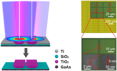
The development of reliable, mass-produced, and cost-effective sub-10 nm nanofabrication technology leads to an unprecedented level of integration of photonic devices. In this work, we describe the development of a laser direct writing (LDW) lithography technique with ∼5 nm feature size, which is about 1/55 of the optical diffraction limit of the LDW system (405 nm laser and 0.9 NA objective), and the realization of 5 nm nanogap electrodes. This LDW lithography exhibits an attractive capability of well-site control and mass production of ∼5 × 10⁵ nanogap electrodes per hour, breaking the trade-off between resolution and throughput in a nanofabrication technique. Nanosensing chips have been demonstrated with the as-obtained nanogap electrodes, where controllable surface enhancement Raman scattering of rhodamine 6G has been realized via adjusting the gap width and, especially, the applied bias voltages. Our results establish that such a low-cost and high-efficient lithography technology has great potential to fabricate compact integrated circuits and biochips.
中文翻译:

超分辨率激光光刻技术制备5 nm纳米间隙电极和阵列。
可靠,批量生产且具有成本效益的10纳米以下纳米制造技术的发展带来了前所未有的光子器件集成水平。在这项工作中,我们描述了特征尺寸约为5 nm的激光直接写入(LDW)光刻技术的发展情况,该技术尺寸约为LDW系统(405 nm激光和0.9 NA物镜)的光学衍射极限的1/55,并实现了5 nm纳米间隙电极。这种LDW光刻技术具有良好的现场控制能力和约5 ×10 5的批量生产能力每小时可加工纳米间隙电极,从而打破了纳米加工技术在分辨率和生产量之间的权衡。纳米感测芯片已经获得了纳米间隙电极的证明,其中罗丹明6G的可控表面增强拉曼散射是通过调节间隙宽度,尤其是施加的偏置电压来实现的。我们的结果证明,这种低成本,高效的光刻技术在制造紧凑的集成电路和生物芯片方面具有巨大的潜力。
更新日期:2020-07-08
中文翻译:
超分辨率激光光刻技术制备5 nm纳米间隙电极和阵列。
可靠,批量生产且具有成本效益的10纳米以下纳米制造技术的发展带来了前所未有的光子器件集成水平。在这项工作中,我们描述了特征尺寸约为5 nm的激光直接写入(LDW)光刻技术的发展情况,该技术尺寸约为LDW系统(405 nm激光和0.9 NA物镜)的光学衍射极限的1/55,并实现了5 nm纳米间隙电极。这种LDW光刻技术具有良好的现场控制能力和约5 ×10 5的批量生产能力每小时可加工纳米间隙电极,从而打破了纳米加工技术在分辨率和生产量之间的权衡。纳米感测芯片已经获得了纳米间隙电极的证明,其中罗丹明6G的可控表面增强拉曼散射是通过调节间隙宽度,尤其是施加的偏置电压来实现的。我们的结果证明,这种低成本,高效的光刻技术在制造紧凑的集成电路和生物芯片方面具有巨大的潜力。


 京公网安备 11010802027423号