当前位置:
X-MOL 学术
›
Diam. Relat. Mater.
›
论文详情
Our official English website, www.x-mol.net, welcomes your feedback! (Note: you will need to create a separate account there.)
Nanoscale profiling of multilayer graphene films on silicon carbide by a focused ion beam
Diamond and Related Materials ( IF 4.1 ) Pub Date : 2020-10-01 , DOI: 10.1016/j.diamond.2020.107969 A.S. Kolomiytsev , I.L. Jityaev , A.M. Svetlichnyi , A.A. Fedotov , O.A. Ageev
Diamond and Related Materials ( IF 4.1 ) Pub Date : 2020-10-01 , DOI: 10.1016/j.diamond.2020.107969 A.S. Kolomiytsev , I.L. Jityaev , A.M. Svetlichnyi , A.A. Fedotov , O.A. Ageev
|
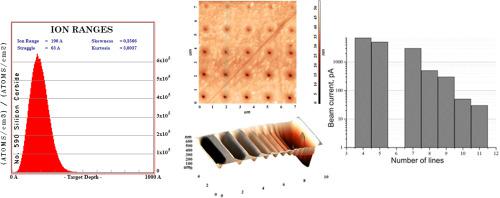
Abstract The controlled and reproducible formation of a nanoscale interelectrode gap is crucial for the development of next-generation nanoelectronics devices, such as nano-electromechanical systems or field emission structures. This paper reports an etching of multilayer graphene (MLG) film on silicon carbide using focused ion beam (Ga+). The main task is to obtain nanoscale width trenches for the formation of isolated planar nanostructures based on MLG. MLG were obtained by thermal decomposition of silicon carbide in vacuum. We used 6H-SiC as a substrate. The analysis of the Raman spectrum showed the presence of about 10 layers of graphene in the film. The influence of the focused ion beam (FIB) parameters on the distribution of the Ga+ ions concentration in the SiC substrate was estimated by the Monte Carlo method. We revealed the maximum concentration of Ga+ ions in the SiC substrate is at a depth of 19 nm at the ion energy of 30 keV and the incidence angle of the ion beam on the substrate relative to the normal 0°. The results of local nanoscale etching of MLG on SiC by using FIB are presented. The AFM-studies confirm the dependence of the geometric dimensions of the etching area on the FIB etching parameters. The resolving power of the method is determined on the basis of a number of detectable nanoscale trenches at various currents of the FIB.
中文翻译:

通过聚焦离子束对碳化硅上的多层石墨烯薄膜进行纳米级分析
摘要 纳米级电极间间隙的可控且可重复的形成对于下一代纳米电子器件的开发至关重要,例如纳米机电系统或场发射结构。本文报道了使用聚焦离子束 (Ga+) 在碳化硅上蚀刻多层石墨烯 (MLG) 膜。主要任务是获得纳米级宽度的沟槽,用于形成基于 MLG 的隔离平面纳米结构。MLG是通过碳化硅在真空中的热分解获得的。我们使用 6H-SiC 作为衬底。拉曼光谱分析表明薄膜中存在约 10 层石墨烯。聚焦离子束 (FIB) 参数对 SiC 衬底中 Ga+ 离子浓度分布的影响通过蒙特卡罗方法进行估计。我们揭示了 SiC 衬底中 Ga+ 离子的最大浓度在 19 nm 的深度处,离子能量为 30 keV,衬底上离子束相对于法线的入射角为 0°。介绍了使用 FIB 在 SiC 上局部纳米级蚀刻 MLG 的结果。AFM 研究证实了蚀刻区域的几何尺寸对 FIB 蚀刻参数的依赖性。该方法的分辨能力是基于在 FIB 的各种电流下可检测到的纳米级沟槽的数量来确定的。AFM 研究证实了蚀刻区域的几何尺寸对 FIB 蚀刻参数的依赖性。该方法的分辨能力是基于在 FIB 的各种电流下可检测到的纳米级沟槽的数量来确定的。AFM 研究证实了蚀刻区域的几何尺寸对 FIB 蚀刻参数的依赖性。该方法的分辨能力是基于在 FIB 的各种电流下可检测到的纳米级沟槽的数量来确定的。
更新日期:2020-10-01
中文翻译:
通过聚焦离子束对碳化硅上的多层石墨烯薄膜进行纳米级分析
摘要 纳米级电极间间隙的可控且可重复的形成对于下一代纳米电子器件的开发至关重要,例如纳米机电系统或场发射结构。本文报道了使用聚焦离子束 (Ga+) 在碳化硅上蚀刻多层石墨烯 (MLG) 膜。主要任务是获得纳米级宽度的沟槽,用于形成基于 MLG 的隔离平面纳米结构。MLG是通过碳化硅在真空中的热分解获得的。我们使用 6H-SiC 作为衬底。拉曼光谱分析表明薄膜中存在约 10 层石墨烯。聚焦离子束 (FIB) 参数对 SiC 衬底中 Ga+ 离子浓度分布的影响通过蒙特卡罗方法进行估计。我们揭示了 SiC 衬底中 Ga+ 离子的最大浓度在 19 nm 的深度处,离子能量为 30 keV,衬底上离子束相对于法线的入射角为 0°。介绍了使用 FIB 在 SiC 上局部纳米级蚀刻 MLG 的结果。AFM 研究证实了蚀刻区域的几何尺寸对 FIB 蚀刻参数的依赖性。该方法的分辨能力是基于在 FIB 的各种电流下可检测到的纳米级沟槽的数量来确定的。AFM 研究证实了蚀刻区域的几何尺寸对 FIB 蚀刻参数的依赖性。该方法的分辨能力是基于在 FIB 的各种电流下可检测到的纳米级沟槽的数量来确定的。AFM 研究证实了蚀刻区域的几何尺寸对 FIB 蚀刻参数的依赖性。该方法的分辨能力是基于在 FIB 的各种电流下可检测到的纳米级沟槽的数量来确定的。


 京公网安备 11010802027423号