当前位置:
X-MOL 学术
›
Micro Nanostruct.
›
论文详情
Our official English website, www.x-mol.net, welcomes your feedback! (Note: you will need to create a separate account there.)
Structural, morphological, compositional, optical and electrical properties of Sb2Se3 thin films deposited by pulsed laser deposition
Micro and Nanostructures ( IF 3.1 ) Pub Date : 2020-09-01 , DOI: 10.1016/j.spmi.2020.106618 Ke Yang , Bing Li , Guanggen Zeng
Micro and Nanostructures ( IF 3.1 ) Pub Date : 2020-09-01 , DOI: 10.1016/j.spmi.2020.106618 Ke Yang , Bing Li , Guanggen Zeng
|
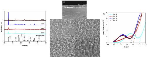
Abstract Sb2Se3 is a promising absorber for thin film solar cells due to its nontoxicity, low cost, earth abundance and excellent photovoltaic properties. However, few reports focus on Sb2Se3 thin films prepared by pulsed laser deposition (PLD). Here we successfully deposited Sb2Se3 thin films at different substrate temperatures by PLD. Structural, morphological, compositional, optical and electrical properties of Sb2Se3 thin films were characterized. Results show that Sb2Se3 thin films exhibit orthorhombic phase with good crystallinity and higher substrate temperature can distinctly improve crystal quality. Optical band gap is about 1.30 eV, 1.20 eV, 1.18 eV and 1.16 eV for Sb2Se3 thin films deposited at 370 °C, 390 °C, 410 °C and 430 °C, respectively. In addition, the atomic ratio of selenium to antimony is 3/2, entirely consistent with the stoichiometry ratio of Sb2Se3.
中文翻译:

通过脉冲激光沉积沉积的 Sb2Se3 薄膜的结构、形态、成分、光学和电学特性
摘要 Sb2Se3 具有无毒、低成本、地球丰度和优异的光伏特性,是一种很有前途的薄膜太阳能电池吸收剂。然而,很少有报道关注通过脉冲激光沉积 (PLD) 制备的 Sb2Se3 薄膜。在这里,我们通过 PLD 在不同的衬底温度下成功地沉积了 Sb2Se3 薄膜。表征了 Sb2Se3 薄膜的结构、形态、成分、光学和电学特性。结果表明,Sb2Se3薄膜呈正交相,结晶度好,较高的衬底温度可以明显提高晶体质量。对于在 370 °C、390 °C、410 °C 和 430 °C 下沉积的 Sb2Se3 薄膜,光学带隙分别约为 1.30 eV、1.20 eV、1.18 eV 和 1.16 eV。此外,硒与锑的原子比为3/2,
更新日期:2020-09-01
中文翻译:
通过脉冲激光沉积沉积的 Sb2Se3 薄膜的结构、形态、成分、光学和电学特性
摘要 Sb2Se3 具有无毒、低成本、地球丰度和优异的光伏特性,是一种很有前途的薄膜太阳能电池吸收剂。然而,很少有报道关注通过脉冲激光沉积 (PLD) 制备的 Sb2Se3 薄膜。在这里,我们通过 PLD 在不同的衬底温度下成功地沉积了 Sb2Se3 薄膜。表征了 Sb2Se3 薄膜的结构、形态、成分、光学和电学特性。结果表明,Sb2Se3薄膜呈正交相,结晶度好,较高的衬底温度可以明显提高晶体质量。对于在 370 °C、390 °C、410 °C 和 430 °C 下沉积的 Sb2Se3 薄膜,光学带隙分别约为 1.30 eV、1.20 eV、1.18 eV 和 1.16 eV。此外,硒与锑的原子比为3/2,


 京公网安备 11010802027423号