当前位置:
X-MOL 学术
›
Adv. Electron. Mater.
›
论文详情
Our official English website, www.x-mol.net, welcomes your feedback! (Note: you will need to create a separate account there.)
Operational Stability Enhancement of Polymeric Organic Field‐Effect Transistors by Amorphous Perfluoropolymers Chemically Anchored to Gate Dielectric Surfaces
Advanced Electronic Materials ( IF 6.2 ) Pub Date : 2020-06-09 , DOI: 10.1002/aelm.202000161 Kirill Bulgarevich 1, 2 , Kenji Sakamoto 1 , Takeshi Yasuda 3 , Takeo Minari 1 , Masayuki Takeuchi 2, 3
Advanced Electronic Materials ( IF 6.2 ) Pub Date : 2020-06-09 , DOI: 10.1002/aelm.202000161 Kirill Bulgarevich 1, 2 , Kenji Sakamoto 1 , Takeshi Yasuda 3 , Takeo Minari 1 , Masayuki Takeuchi 2, 3
Affiliation
|
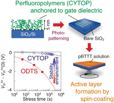
Bias‐stress resistance of polymer‐based organic field‐effect transistors (OFETs) is considerably enhanced by coating the gate dielectric surface with an amorphous perfluoropolymer (CYTOP). In bottom‐gate (BG) OFETs offering a relatively simple fabrication process, the CYTOP coating causes a serious problem; that is, thin film formation of organic semiconducting polymers generally fails due to the lyophobic properties of CYTOP. This problem is solved by patterning the CYTOP coating layer with suitable designs. Here, a simple photo‐patterning method is established using CYTOP terminated with amidosilyl functional groups. This method is composed of self‐limited thinning process of CYTOP coating layers, exposure to vacuum ultraviolet light through a photomask, and development. BG/top‐contact OFET arrays are fabricated using poly(2,5‐bis(3‐hexadecylthiophene‐2‐yl)thieno[3,2‐b]thiophene) as the semiconducting polymer. The initial electrical properties and bias‐stress resistance are compared with those of OFETs with octadecyltrichlorosilane (ODTS)‐treated gate dielectrics. The CYTOP‐ and ODTS‐OFETs show approximately the same initial electrical properties with very small device‐to‐device variation, while the CYTOP‐OFETs exhibit much higher intrinsic bias‐stress resistance. Therefore, the spin‐coating combined with the simple photo‐patterning method is a promising technique that can form polymeric organic semiconductor layers on CYTOP layers and produce BG OFETs exhibiting very high operational stability.
中文翻译:

化学固定在栅介电表面上的非晶全氟聚合物可增强聚合物有机场效应晶体管的工作稳定性
聚合物基有机场效应晶体管(OFET)的耐偏应力性通过用非晶全氟聚合物(CYTOP)覆盖栅极电介质表面而大大提高。在底栅(BG)OFET提供相对简单的制造工艺的情况下,CYTOP涂层会引起严重的问题。也就是说,由于CYTOP的疏液性,有机半导体聚合物的薄膜形成通常会失败。通过用合适的设计图案化CYTOP涂层解决了这个问题。在这里,使用以氨基甲硅烷基官能团封端的CYTOP建立了一种简单的光图案化方法。该方法由CYTOP涂层的自限薄化工艺,通过光掩模暴露于真空紫外光以及显影组成。BG /顶部接触式OFET阵列是使用poly(2,5-双(3-十六烷基噻吩-2-基)噻吩并[3,2-b]噻吩)作为半导体聚合物。将初始电性能和抗偏应力性能与经过十八烷基三氯硅烷(ODTS)处理的栅极电介质的OFET进行比较。CYTOP‐和ODTS‐OFET表现出几乎相同的初始电特性,并且器件之间的差异非常小,而CYTOP‐OFET则表现出更高的固有偏置耐压性。因此,将旋涂与简单的光图案化方法相结合是一种很有前途的技术,可以在CYTOP层上形成聚合物有机半导体层,并生产出具有非常高的操作稳定性的BG OFET。将初始电性能和抗偏应力性能与经十八烷基三氯硅烷(ODTS)处理的栅极电介质的OFET进行比较。CYTOP‐和ODTS‐OFET的初始电学性质几乎相同,器件间差异很小,而CYTOP‐OFET的固有耐偏应力性要高得多。因此,将旋涂与简单的光图案化方法相结合是一种很有前途的技术,可以在CYTOP层上形成聚合物有机半导体层,并生产出具有非常高的操作稳定性的BG OFET。将初始电性能和抗偏应力性能与经过十八烷基三氯硅烷(ODTS)处理的栅极电介质的OFET进行比较。CYTOP‐和ODTS‐OFET的初始电学性质几乎相同,器件间差异很小,而CYTOP‐OFET的固有耐偏应力性要高得多。因此,将旋涂与简单的光图案化方法相结合是一种很有前途的技术,可以在CYTOP层上形成聚合物有机半导体层,并生产出具有非常高的操作稳定性的BG OFET。
更新日期:2020-07-13
中文翻译:
化学固定在栅介电表面上的非晶全氟聚合物可增强聚合物有机场效应晶体管的工作稳定性
聚合物基有机场效应晶体管(OFET)的耐偏应力性通过用非晶全氟聚合物(CYTOP)覆盖栅极电介质表面而大大提高。在底栅(BG)OFET提供相对简单的制造工艺的情况下,CYTOP涂层会引起严重的问题。也就是说,由于CYTOP的疏液性,有机半导体聚合物的薄膜形成通常会失败。通过用合适的设计图案化CYTOP涂层解决了这个问题。在这里,使用以氨基甲硅烷基官能团封端的CYTOP建立了一种简单的光图案化方法。该方法由CYTOP涂层的自限薄化工艺,通过光掩模暴露于真空紫外光以及显影组成。BG /顶部接触式OFET阵列是使用poly(2,5-双(3-十六烷基噻吩-2-基)噻吩并[3,2-b]噻吩)作为半导体聚合物。将初始电性能和抗偏应力性能与经过十八烷基三氯硅烷(ODTS)处理的栅极电介质的OFET进行比较。CYTOP‐和ODTS‐OFET表现出几乎相同的初始电特性,并且器件之间的差异非常小,而CYTOP‐OFET则表现出更高的固有偏置耐压性。因此,将旋涂与简单的光图案化方法相结合是一种很有前途的技术,可以在CYTOP层上形成聚合物有机半导体层,并生产出具有非常高的操作稳定性的BG OFET。将初始电性能和抗偏应力性能与经十八烷基三氯硅烷(ODTS)处理的栅极电介质的OFET进行比较。CYTOP‐和ODTS‐OFET的初始电学性质几乎相同,器件间差异很小,而CYTOP‐OFET的固有耐偏应力性要高得多。因此,将旋涂与简单的光图案化方法相结合是一种很有前途的技术,可以在CYTOP层上形成聚合物有机半导体层,并生产出具有非常高的操作稳定性的BG OFET。将初始电性能和抗偏应力性能与经过十八烷基三氯硅烷(ODTS)处理的栅极电介质的OFET进行比较。CYTOP‐和ODTS‐OFET的初始电学性质几乎相同,器件间差异很小,而CYTOP‐OFET的固有耐偏应力性要高得多。因此,将旋涂与简单的光图案化方法相结合是一种很有前途的技术,可以在CYTOP层上形成聚合物有机半导体层,并生产出具有非常高的操作稳定性的BG OFET。


 京公网安备 11010802027423号