当前位置:
X-MOL 学术
›
Adv. Electron. Mater.
›
论文详情
Our official English website, www.x-mol.net, welcomes your feedback! (Note: you will need to create a separate account there.)
n‐Type Dirac‐Source Field‐Effect Transistors Based on a Graphene/Carbon Nanotube Heterojunction
Advanced Electronic Materials ( IF 6.2 ) Pub Date : 2020-06-09 , DOI: 10.1002/aelm.202000258 Mengmeng Xiao 1 , Yanxia Lin 2 , Lin Xu 1 , Bing Deng 3 , Hailin Peng 3 , Lian‐Mao Peng 1 , Zhiyong Zhang 1
Advanced Electronic Materials ( IF 6.2 ) Pub Date : 2020-06-09 , DOI: 10.1002/aelm.202000258 Mengmeng Xiao 1 , Yanxia Lin 2 , Lin Xu 1 , Bing Deng 3 , Hailin Peng 3 , Lian‐Mao Peng 1 , Zhiyong Zhang 1
Affiliation
|
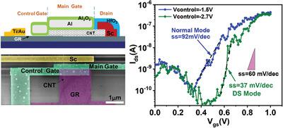
As a type of steep‐slope transistor, a Dirac‐source field‐effect transistor (DS‐FET) provides both high performance and sub‐60 mV dec−1 subthreshold swing (SS) at room temperature. However, only p‐type DS‐FETs are experimentally demonstrated, and n‐type DS‐FETs for constructing complementary metal–oxide–semiconductor (CMOS) logic circuits are lacking. Here, the first experimental demonstrations of n‐type DS‐FETs and tunneling FETs (TFETs) based on a graphene/carbon nanotube heterojunction with a Sc drain are provided. The as‐fabricated n‐type DS‐FETs present a minimum SS as low as 37 mV dec−1 at room temperature and a high I 60 of 2.6 µA µm−1 (V ds = 0.1 V), which reflect an advantage in the on‐state performance of more than two orders of magnitude over the TFETs. In addition, the G m/I ds ratio reaches 70 V−1, which breaks the physical limit (38.5 V−1) and reflects the ultrahigh transconductance efficiency of the transistor for analog applications. The realization of n‐type DS‐FETs not only opens a door to achieving CMOS DS‐FETs for future high‐energy‐efficiency digital electronics and high‐performance analog electronics but also further verifies the validity and universality of device physics for DS‐FETs.
中文翻译:

基于石墨烯/碳纳米管异质结的n型Dirac源场效应晶体管
作为一种陡坡晶体管,狄拉克源场效应晶体管(DS-FET )在室温下可提供高性能和低于60 mV dec -1的亚阈值摆幅(SS)。但是,仅通过实验证明了p型DS-FET,而缺少用于构造互补金属氧化物半导体(CMOS)逻辑电路的n型DS-FET。在此,提供了基于具有Sc漏的石墨烯/碳纳米管异质结的n型DS-FET和隧道FET(TFET)的首次实验演示。制成的n型DS-FET在室温下的最小SS低至37 mV dec -1,I 60高达2.6 µA µm -1(V ds= 0.1 V),这反映了导通性能比TFET高两个数量级以上的优势。此外,G m / I ds比达到70 V -1,这打破了物理极限(38.5 V -1),反映了模拟应用晶体管的超高跨导效率。n型DS-FET的实现不仅为实现将来的高能效数字电子产品和高性能模拟电子产品的CMOS DS-FET打开了一扇门,而且进一步验证了DS-FET的器件物理性的有效性和普遍性。
更新日期:2020-07-13
中文翻译:
基于石墨烯/碳纳米管异质结的n型Dirac源场效应晶体管
作为一种陡坡晶体管,狄拉克源场效应晶体管(DS-FET )在室温下可提供高性能和低于60 mV dec -1的亚阈值摆幅(SS)。但是,仅通过实验证明了p型DS-FET,而缺少用于构造互补金属氧化物半导体(CMOS)逻辑电路的n型DS-FET。在此,提供了基于具有Sc漏的石墨烯/碳纳米管异质结的n型DS-FET和隧道FET(TFET)的首次实验演示。制成的n型DS-FET在室温下的最小SS低至37 mV dec -1,I 60高达2.6 µA µm -1(V ds= 0.1 V),这反映了导通性能比TFET高两个数量级以上的优势。此外,G m / I ds比达到70 V -1,这打破了物理极限(38.5 V -1),反映了模拟应用晶体管的超高跨导效率。n型DS-FET的实现不仅为实现将来的高能效数字电子产品和高性能模拟电子产品的CMOS DS-FET打开了一扇门,而且进一步验证了DS-FET的器件物理性的有效性和普遍性。


 京公网安备 11010802027423号