当前位置:
X-MOL 学术
›
Nano Lett.
›
论文详情
Our official English website, www.x-mol.net, welcomes your feedback! (Note: you will need to create a separate account there.)
Realization of ∼10 nm Features on Semiconductor Surfaces via Femtosecond Laser Direct Patterning in Far Field and in Ambient Air.
Nano Letters ( IF 10.8 ) Pub Date : 2020-06-08 , DOI: 10.1021/acs.nanolett.0c01013 Zhenyuan Lin 1, 2, 3 , Huagang Liu 1 , Lingfei Ji 2, 3 , Wenxiong Lin 4 , Minghui Hong 1
Nano Letters ( IF 10.8 ) Pub Date : 2020-06-08 , DOI: 10.1021/acs.nanolett.0c01013 Zhenyuan Lin 1, 2, 3 , Huagang Liu 1 , Lingfei Ji 2, 3 , Wenxiong Lin 4 , Minghui Hong 1
Affiliation
|
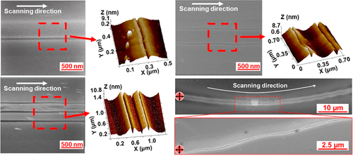
Direct fabrication of ∼10 nm features by optical means in far field and in ambient air on semiconductor surfaces is significant for next-generation advances nanomanufacturing. We report here a new method that enables the direct formation of 12 nm (λ/66) features on silicon surfaces. It is processed in far field and in ambient air via the irradiation of orthogonally polarized double femtosecond laser beams. The coupling of orthogonally polarized double femtosecond laser beams and the incubation effect due to multiple femtosecond laser pulses irradiation under high repetition rate enable the 12 nm nanostructures creation parallel to the scanning direction, regardless of scanning path.
中文翻译:

通过飞秒激光直接图案化在远场和环境空气中在半导体表面上实现约10 nm的特性。
通过光学手段在远场和环境空气中在半导体表面上直接制造约10 nm的特征对于下一代先进的纳米制造意义重大。我们在这里报告了一种新方法,该方法能够在硅表面上直接形成12 nm(λ/ 66)特征。通过正交偏振双飞秒激光束的照射,可以在远场和环境空气中对其进行处理。正交偏振双飞秒激光束的耦合以及由于在高重复率下多次飞秒激光脉冲辐照而产生的孵化效果,无论扫描路径如何,均可产生平行于扫描方向的12 nm纳米结构。
更新日期:2020-07-08
中文翻译:
通过飞秒激光直接图案化在远场和环境空气中在半导体表面上实现约10 nm的特性。
通过光学手段在远场和环境空气中在半导体表面上直接制造约10 nm的特征对于下一代先进的纳米制造意义重大。我们在这里报告了一种新方法,该方法能够在硅表面上直接形成12 nm(λ/ 66)特征。通过正交偏振双飞秒激光束的照射,可以在远场和环境空气中对其进行处理。正交偏振双飞秒激光束的耦合以及由于在高重复率下多次飞秒激光脉冲辐照而产生的孵化效果,无论扫描路径如何,均可产生平行于扫描方向的12 nm纳米结构。


 京公网安备 11010802027423号