当前位置:
X-MOL 学术
›
Adv. Electron. Mater.
›
论文详情
Our official English website, www.x-mol.net, welcomes your feedback! (Note: you will need to create a separate account there.)
Origin of the Threshold Voltage Shift in a Transistor with a 2D Electron Gas Channel at the Al2O3/SrTiO3 Interface
Advanced Electronic Materials ( IF 6.2 ) Pub Date : 2020-05-08 , DOI: 10.1002/aelm.201901286 Taehwan Moon 1 , Hyun Jae Lee 1 , Seung Dam Hyun 1 , Baek Su Kim 1 , Ho Hyun Kim 1 , Cheol Seong Hwang 1
Advanced Electronic Materials ( IF 6.2 ) Pub Date : 2020-05-08 , DOI: 10.1002/aelm.201901286 Taehwan Moon 1 , Hyun Jae Lee 1 , Seung Dam Hyun 1 , Baek Su Kim 1 , Ho Hyun Kim 1 , Cheol Seong Hwang 1
Affiliation
|
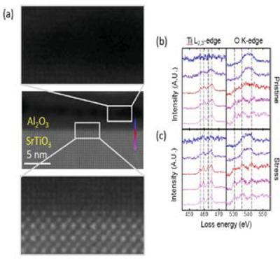
A transistor is fabricated with a 2D electron gas (2DEG) channel at the Al2O3 (AO)/SrTiO3 (STO) interface. The threshold voltage (V th) shift of the 2DEG channel in the Pt/AO/2DEG/STO stack induced by negative bias stress is investigated. Two‐terminal current–voltage and capacitance–voltage characterization through the gate and the source reveals that the metallic 2DEG channel turns into a semiconducting channel when the negative bias stress is applied. Transfer curve measurement with various stress conditions on the 2DEG field‐effect transistor is performed to evaluate the effect of the negative bias stress. The V th becomes positive, and the channel conductance decreases after the application of negative bias stress. These variations are promoted by large stress bias and temperature. Electron energy loss spectroscopy analysis via scanning transmission electron microscopy reveals that the chemical state of the interface changes from oxygen‐deficient to stoichiometric. Therefore, the change in the channel state from metallic to semiconducting originates from the decrease of oxygen vacancy concentration at the interface.
中文翻译:

Al2O3 / SrTiO3界面上带有2D电子气通道的晶体管的阈值电压漂移的起因
用在Al 2 O 3(AO)/ SrTiO 3(STO)界面的2D电子气(2DEG)通道制造晶体管。研究了由负偏置应力引起的Pt / AO / 2DEG / STO堆栈中2DEG通道的阈值电压(V th)的变化。通过栅极和源极的两端电流-电压和电容-电压表征表明,施加负偏置应力后,金属2DEG通道变成了半导体通道。在2DEG场效应晶体管上使用各种应力条件进行传递曲线测量,以评估负偏置应力的影响。该V日变为正值后,施加负偏置应力后沟道电导减小。较大的应力偏差和温度会促进这些变化。通过扫描透射电子显微镜进行的电子能量损失光谱分析表明,界面的化学状态从缺氧变为化学计量。因此,通道状态从金属到半导体的变化源于界面处氧空位浓度的降低。
更新日期:2020-05-08
中文翻译:
Al2O3 / SrTiO3界面上带有2D电子气通道的晶体管的阈值电压漂移的起因
用在Al 2 O 3(AO)/ SrTiO 3(STO)界面的2D电子气(2DEG)通道制造晶体管。研究了由负偏置应力引起的Pt / AO / 2DEG / STO堆栈中2DEG通道的阈值电压(V th)的变化。通过栅极和源极的两端电流-电压和电容-电压表征表明,施加负偏置应力后,金属2DEG通道变成了半导体通道。在2DEG场效应晶体管上使用各种应力条件进行传递曲线测量,以评估负偏置应力的影响。该V日变为正值后,施加负偏置应力后沟道电导减小。较大的应力偏差和温度会促进这些变化。通过扫描透射电子显微镜进行的电子能量损失光谱分析表明,界面的化学状态从缺氧变为化学计量。因此,通道状态从金属到半导体的变化源于界面处氧空位浓度的降低。


 京公网安备 11010802027423号