当前位置:
X-MOL 学术
›
Phys. Status Solidi B
›
论文详情
Our official English website, www.x-mol.net, welcomes your feedback! (Note: you will need to create a separate account there.)
Theoretical Analysis of Strain‐Optoelectronic Properties in Externally Deformed Ge/GeSi Quantum Well Nanomembranes via Neutral Plane Modulation
Physica Status Solidi (B) - Basic Solid State Physics ( IF 1.6 ) Pub Date : 2020-05-06 , DOI: 10.1002/pssb.201900732 Jiushuang Zhang 1, 2, 3 , Yun Xu 1, 2, 3 , Weitong Wu 1, 2, 3 , Wei Lu 1, 2, 3 , Guofeng Song 1, 2, 3
Physica Status Solidi (B) - Basic Solid State Physics ( IF 1.6 ) Pub Date : 2020-05-06 , DOI: 10.1002/pssb.201900732 Jiushuang Zhang 1, 2, 3 , Yun Xu 1, 2, 3 , Weitong Wu 1, 2, 3 , Wei Lu 1, 2, 3 , Guofeng Song 1, 2, 3
Affiliation
|
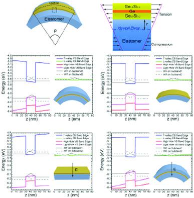
For indirect‐bandgap germanium (Ge), strain‐engineering provides a controllable means to transform Ge into direct‐bandgap material with strongly enhanced light emission efficiency. Flexible electronics offer a powerful platform for introducing external strain into semiconductor nanomembranes (NMs) through deformation with flexible substrates. So far, the Ge/GexSi1−x alloy quantum well (QW) NMs have not been sufficiently investigated to comprehend how the external deformation tunes the wavelength and light‐emitting properties. Herein, a theoretical model based on the elasticity theory and k·p method is established to analyze the strain‐optoelectronic properties of the externally deformed Ge/GexSi1−x QW NMs via neutral plane (NP) modulation in both embedded and sticked form. Calculated results reveal that the elastic strain is linearly distributed, inducing tilt of the band edge similar to the electric field. Considering the fracture limit of the material, the NP layout determines the critical bending curvature that the NM can achieve. Large tunable range of wavelength Δλ of 1615 nm and enhanced transverse electric (TE)/transverse magnetic (TM) peak gain of 949/3778 cm−1 are predicted for r = 1000 nm (the distance between NP and QW) under the bending limit. Further calculations conclude that larger r allow for smaller bending curvature to achieve wider range of wavelength and more enhanced optical gain.
中文翻译:

中性面调制对外部形变Ge / GeSi量子阱纳米膜的应变光电特性的理论分析
对于间接带隙锗(Ge),应变工程提供了一种可控制的方法,可将Ge转换为具有直接增强的发光效率的直接带隙材料。柔性电子器件提供了一个强大的平台,可通过柔性衬底的变形将外部应变引入半导体纳米膜(NMs)。迄今为止,尚未充分研究Ge / Ge x Si 1- x合金量子阱(QW)NM,以了解外部变形如何调节波长和发光特性。在此,建立了基于弹性理论和k·p方法的理论模型,以分析外部变形的Ge / Ge x Si 1−的应变光电特性。X QW NMS通过在嵌入式和粘形式中性平面(NP)调制。计算结果表明,弹性应变呈线性分布,导致带边缘倾斜,类似于电场。考虑到材料的断裂极限,NP布局确定了NM可以达到的临界弯曲曲率。波长Δ的大范围的可调谐λ的1615 nm和增强的横向电场(TE)/横向磁(TM)峰的三千七百七十八分之九百四十九厘米增益-1被预测为ř 下弯曲= 1000纳米(NP和QW之间的距离)限制。进一步的计算得出结论,较大的r允许较小的弯曲曲率,以实现更宽的波长范围和更大的光学增益。
更新日期:2020-05-06
中文翻译:
中性面调制对外部形变Ge / GeSi量子阱纳米膜的应变光电特性的理论分析
对于间接带隙锗(Ge),应变工程提供了一种可控制的方法,可将Ge转换为具有直接增强的发光效率的直接带隙材料。柔性电子器件提供了一个强大的平台,可通过柔性衬底的变形将外部应变引入半导体纳米膜(NMs)。迄今为止,尚未充分研究Ge / Ge x Si 1- x合金量子阱(QW)NM,以了解外部变形如何调节波长和发光特性。在此,建立了基于弹性理论和k·p方法的理论模型,以分析外部变形的Ge / Ge x Si 1−的应变光电特性。X QW NMS通过在嵌入式和粘形式中性平面(NP)调制。计算结果表明,弹性应变呈线性分布,导致带边缘倾斜,类似于电场。考虑到材料的断裂极限,NP布局确定了NM可以达到的临界弯曲曲率。波长Δ的大范围的可调谐λ的1615 nm和增强的横向电场(TE)/横向磁(TM)峰的三千七百七十八分之九百四十九厘米增益-1被预测为ř 下弯曲= 1000纳米(NP和QW之间的距离)限制。进一步的计算得出结论,较大的r允许较小的弯曲曲率,以实现更宽的波长范围和更大的光学增益。


 京公网安备 11010802027423号