当前位置:
X-MOL 学术
›
Micro Nanostruct.
›
论文详情
Our official English website, www.x-mol.net, welcomes your feedback! (Note: you will need to create a separate account there.)
Carrier transport of rough-edged doped GNRFETs with metal contacts at various channel widths
Micro and Nanostructures ( IF 3.1 ) Pub Date : 2020-07-01 , DOI: 10.1016/j.spmi.2020.106548 Kien Liong Wong , Mu Wen Chuan , Afiq Hamzah , Shahrizal Rusli , Nurul Ezaila Alias , Suhana Mohamed Sultan , Cheng Siong Lim , Michael Loong Peng Tan
Micro and Nanostructures ( IF 3.1 ) Pub Date : 2020-07-01 , DOI: 10.1016/j.spmi.2020.106548 Kien Liong Wong , Mu Wen Chuan , Afiq Hamzah , Shahrizal Rusli , Nurul Ezaila Alias , Suhana Mohamed Sultan , Cheng Siong Lim , Michael Loong Peng Tan
|
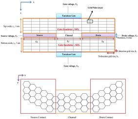
Abstract Graphene nanoribbons (GNRs) have attracted much attention owing to their exotic electronic properties. However, it is impossible to fabricate GNRs with perfect edges. The edge roughness effect will degrade the performance of the field effect transistor (FET). Therefore, modelling GNR FETs (GNRFETs) with the line-edge roughness effect and doping is crucial for evaluating the performance metrics of these devices. In this research study, the carrier transport properties of double-gate, monolayer, doped, rough-edged armchair GNRFETs (AGNRFETs) with various channel widths, and metallic zigzag GNR (ZGNR) contacts are studied. The investigated width index originates from the 3p+1 family, and step and edge doping with nitrogen atoms (n-doping) and boron atoms (p-doping) are applied. In addition, the nearest-neighbour tight-binding method is employed to build the Hamiltonian matrix of the device. The self-consistent solutions of the Poisson and Schrodinger equations are computed with the recursive non-equilibrium Green's function (NEGF) method and successive over-relaxation (SOR) method to minimise the time consumption for convergence. The carrier transport properties of the pristine and non-pristine devices (e.g. the total density of states (DOS), transmission coefficient, energy-resolved current spectrum, and various current–voltage characteristics) are simulated. Based on the output, the performance metrics of the device, including the subthreshold swing, drain-induced barrier lowering (DIBL), threshold voltage, and on/off current ratio, are calculated. The results of different widths are compared separately and for the pristine and doped rough-edged channel devices. For narrower devices, the subthreshold swing and DIBL decrease, whereas the threshold voltage and on/off current ratio increase. The subthreshold swing and DIBL of the doped rough-edged channel device are superior to those of the pristine channel device. Moreover, the on-current, threshold voltage, and on/off current ratio of the rough-edged channel improve with dopants. N-doping achieves a much higher current in the on-state owing to the lighter electron mass and faster electron velocity compared with those of holes. Furthermore, the n-type rough-edged seven-armchair GNRFET with a length of 5 nm exhibits an outstanding subthreshold swing of approximately 85.2 mV/dec and a DIBL of 63.03 mV/V. Thereby, the narrower doped, rough-edged device is less affected by short-channel effects and exhibits lower leakage currents in the off-state. This results in a better switching performance, which makes it a potential candidate for future nano-electronic applications with low-power design.
中文翻译:

具有不同沟道宽度的金属触点的粗糙边缘掺杂 GNRFET 的载流子传输
摘要 石墨烯纳米带(GNRs)因其奇异的电子特性而备受关注。然而,不可能制造出具有完美边缘的 GNR。边缘粗糙度效应会降低场效应晶体管 (FET) 的性能。因此,使用线边缘粗糙度效应和掺杂对 GNR FET (GNRFET) 进行建模对于评估这些器件的性能指标至关重要。在这项研究中,研究了具有各种沟道宽度的双栅极、单层、掺杂、粗糙边缘扶手椅 GNRFET (AGNRFET) 和金属锯齿形 GNR (ZGNR) 触点的载流子传输特性。研究的宽度指数源自 3p+1 系列,并应用了氮原子(n 掺杂)和硼原子(p 掺杂)的阶梯和边缘掺杂。此外,采用最近邻紧束缚方法来构建器件的哈密顿矩阵。Poisson 和 Schrodinger 方程的自洽解是用递归非平衡格林函数 (NEGF) 方法和连续过松弛 (SOR) 方法计算的,以最大限度地减少收敛的时间消耗。模拟了原始和非原始器件的载流子传输特性(例如总态密度 (DOS)、传输系数、能量分辨电流谱和各种电流-电压特性)。根据输出,计算器件的性能指标,包括亚阈值摆幅、漏极感应势垒降低 (DIBL)、阈值电压和开/关电流比。分别比较了原始和掺杂粗边沟道器件的不同宽度的结果。对于较窄的器件,亚阈值摆幅和 DIBL 降低,而阈值电压和开/关电流比增加。掺杂粗边沟道器件的亚阈值摆幅和DIBL优于原始沟道器件的亚阈值摆幅和DIBL。此外,粗糙边缘沟道的导通电流、阈值电压和开/关电流比随掺杂剂而改善。由于与空穴相比更轻的电子质量和更快的电子速度,N 掺杂在导通状态下实现了更高的电流。此外,长度为 5 nm 的 n 型粗边七臂椅 GNRFET 具有约 85.2 mV/dec 的出色亚阈值摆幅和 63.03 mV/V 的 DIBL。因此,较窄的掺杂,粗糙边缘器件受短沟道效应的影响较小,并且在关断状态下具有较低的漏电流。这导致更好的开关性能,这使其成为具有低功耗设计的未来纳米电子应用的潜在候选者。
更新日期:2020-07-01
中文翻译:
具有不同沟道宽度的金属触点的粗糙边缘掺杂 GNRFET 的载流子传输
摘要 石墨烯纳米带(GNRs)因其奇异的电子特性而备受关注。然而,不可能制造出具有完美边缘的 GNR。边缘粗糙度效应会降低场效应晶体管 (FET) 的性能。因此,使用线边缘粗糙度效应和掺杂对 GNR FET (GNRFET) 进行建模对于评估这些器件的性能指标至关重要。在这项研究中,研究了具有各种沟道宽度的双栅极、单层、掺杂、粗糙边缘扶手椅 GNRFET (AGNRFET) 和金属锯齿形 GNR (ZGNR) 触点的载流子传输特性。研究的宽度指数源自 3p+1 系列,并应用了氮原子(n 掺杂)和硼原子(p 掺杂)的阶梯和边缘掺杂。此外,采用最近邻紧束缚方法来构建器件的哈密顿矩阵。Poisson 和 Schrodinger 方程的自洽解是用递归非平衡格林函数 (NEGF) 方法和连续过松弛 (SOR) 方法计算的,以最大限度地减少收敛的时间消耗。模拟了原始和非原始器件的载流子传输特性(例如总态密度 (DOS)、传输系数、能量分辨电流谱和各种电流-电压特性)。根据输出,计算器件的性能指标,包括亚阈值摆幅、漏极感应势垒降低 (DIBL)、阈值电压和开/关电流比。分别比较了原始和掺杂粗边沟道器件的不同宽度的结果。对于较窄的器件,亚阈值摆幅和 DIBL 降低,而阈值电压和开/关电流比增加。掺杂粗边沟道器件的亚阈值摆幅和DIBL优于原始沟道器件的亚阈值摆幅和DIBL。此外,粗糙边缘沟道的导通电流、阈值电压和开/关电流比随掺杂剂而改善。由于与空穴相比更轻的电子质量和更快的电子速度,N 掺杂在导通状态下实现了更高的电流。此外,长度为 5 nm 的 n 型粗边七臂椅 GNRFET 具有约 85.2 mV/dec 的出色亚阈值摆幅和 63.03 mV/V 的 DIBL。因此,较窄的掺杂,粗糙边缘器件受短沟道效应的影响较小,并且在关断状态下具有较低的漏电流。这导致更好的开关性能,这使其成为具有低功耗设计的未来纳米电子应用的潜在候选者。


 京公网安备 11010802027423号