当前位置:
X-MOL 学术
›
Microelectron. Eng.
›
论文详情
Our official English website, www.x-mol.net, welcomes your feedback! (Note: you will need to create a separate account there.)
Effect of deposition angle on fabrication of plasmonic gold nanocones and nanodiscs
Microelectronic Engineering ( IF 2.3 ) Pub Date : 2020-05-01 , DOI: 10.1016/j.mee.2020.111326 Jiří Liška , Filip Ligmajer , Pedro V. Pinho N. , Lukáš Kejík , Michal Kvapil , Petr Dvořák , Michal Horký , Nikolaus S. Leitner , Erik Reimhult , Tomáš Šikola
Microelectronic Engineering ( IF 2.3 ) Pub Date : 2020-05-01 , DOI: 10.1016/j.mee.2020.111326 Jiří Liška , Filip Ligmajer , Pedro V. Pinho N. , Lukáš Kejík , Michal Kvapil , Petr Dvořák , Michal Horký , Nikolaus S. Leitner , Erik Reimhult , Tomáš Šikola
|
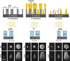
Abstract Metal nanocones can exhibit several strong plasmonic resonances, which are associated with intense and accessible electromagnetic hot spots. They can thus be used to enhance light–matter interactions or to facilitate location-specific sensing while enabling separation of some non-specific contributions towards the sensing signal. Nanocones and similar 3D structures are often fabricated with the use of the so-called self-shading effect, which occurs during the evaporation of a metal film into circular nanowells. Unfortunately, a full description of a successful deposition process with all the essential details is currently missing in literature. Here we present a detailed view of the fabrication of ordered arrays of conical gold nanostructures using electron beam lithography and gold electron beam evaporation. We show that the symmetry of the fabricated nanostructures is influenced by the lateral position of the substrate on the sample holder during the deposition. Off-axis deposition or tilt of the sample leads to asymmetric nanostructures. When the deposited film is thick enough, or the nanowells narrow enough, the entrance aperture is clogged, and nanocones with sharp tips are formed. In contrast, flat-top truncated cones are produced for thinner films or wider nanowells. All these findings help to identify inherent limits for the production of wafer-scale arrays of such non-planar nanostructures. On the other hand, they also suggest new fabrication possibilities for more complicated structures such as mutually connected nanocones for electrically addressable chips.
中文翻译:

沉积角度对等离子体金纳米锥和纳米盘制备的影响
摘要 金属纳米锥可以表现出几种强烈的等离子体共振,这些共振与强烈且可接近的电磁热点有关。因此,它们可用于增强光与物质的相互作用或促进特定位置的传感,同时能够分离对传感信号的一些非特定贡献。纳米锥和类似的 3D 结构通常使用所谓的自阴影效应制造,这种效应发生在金属膜蒸发成圆形纳米井的过程中。不幸的是,目前文献中缺少对成功沉积过程以及所有基本细节的完整描述。在这里,我们详细介绍了使用电子束光刻和金电子束蒸发制造锥形金纳米结构有序阵列的详细视图。我们表明制造的纳米结构的对称性受沉积过程中基板在样品架上的横向位置的影响。样品的离轴沉积或倾斜会导致不对称的纳米结构。当沉积的薄膜足够厚,或者纳米井足够窄时,入口孔就会被堵塞,并形成尖端尖的纳米锥。相比之下,平顶截锥用于更薄的薄膜或更宽的纳米井。所有这些发现都有助于确定生产这种非平面纳米结构的晶片级阵列的固有限制。另一方面,他们还提出了更复杂结构的新制造可能性,例如用于电寻址芯片的相互连接的纳米锥。
更新日期:2020-05-01
中文翻译:
沉积角度对等离子体金纳米锥和纳米盘制备的影响
摘要 金属纳米锥可以表现出几种强烈的等离子体共振,这些共振与强烈且可接近的电磁热点有关。因此,它们可用于增强光与物质的相互作用或促进特定位置的传感,同时能够分离对传感信号的一些非特定贡献。纳米锥和类似的 3D 结构通常使用所谓的自阴影效应制造,这种效应发生在金属膜蒸发成圆形纳米井的过程中。不幸的是,目前文献中缺少对成功沉积过程以及所有基本细节的完整描述。在这里,我们详细介绍了使用电子束光刻和金电子束蒸发制造锥形金纳米结构有序阵列的详细视图。我们表明制造的纳米结构的对称性受沉积过程中基板在样品架上的横向位置的影响。样品的离轴沉积或倾斜会导致不对称的纳米结构。当沉积的薄膜足够厚,或者纳米井足够窄时,入口孔就会被堵塞,并形成尖端尖的纳米锥。相比之下,平顶截锥用于更薄的薄膜或更宽的纳米井。所有这些发现都有助于确定生产这种非平面纳米结构的晶片级阵列的固有限制。另一方面,他们还提出了更复杂结构的新制造可能性,例如用于电寻址芯片的相互连接的纳米锥。


 京公网安备 11010802027423号