当前位置:
X-MOL 学术
›
Microelectron. Eng.
›
论文详情
Our official English website, www.x-mol.net, welcomes your feedback! (Note: you will need to create a separate account there.)
Cryogenic etching for pattern transfer into silicon of Mix-and-Match structured resist layers
Microelectronic Engineering ( IF 2.3 ) Pub Date : 2020-04-01 , DOI: 10.1016/j.mee.2020.111325 Laura Weidenfeller , Martin Hofmann , Shraddha Supreeti , Stephan Mechold , Mathias Holz , Christoph Reuter , Eberhard Manske , Ivo W. Rangelow
Microelectronic Engineering ( IF 2.3 ) Pub Date : 2020-04-01 , DOI: 10.1016/j.mee.2020.111325 Laura Weidenfeller , Martin Hofmann , Shraddha Supreeti , Stephan Mechold , Mathias Holz , Christoph Reuter , Eberhard Manske , Ivo W. Rangelow
|
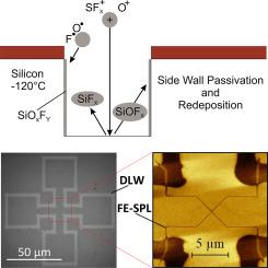
Abstract A Mix-and-Match lithography method for a high-resolution, high-precision and cost effective lithography tool using DLW and FE-SPL was developed and successfully realized. The pattern transfer from the photoresist to the silicon substrate is done by so-called “cryogenic etching”. It means that the substrate is cooled down to cryogenic temperatures. In contrast to etching processes at standard room temperature, the cryogenic temperatures (below −100 °C) enable a highly anisotropic etching process. The difference between etching at room temperature compared to cryogenic etching is carried out in this work. The advantages of the etching process are highlighted for the pattern transfer from Mix-and-Match-structured samples. Therefore, the used photoresist mr-P 1201LIL (microresist technologies GmbH) has been examined concerning its silicon-to-resist selectivity which could be determined to be 6:1 for the applied etching recipe. Using cryogenic etching, we are now able to transfer the Mix-and-Match-structured patterns into silicon with appreciable high selectivities. This opens a novel pathway for the manufacturing of quantum devices on large wafers. The paper discusses current research results based on the TU Ilmenau Nanopositioning and Nanomeasuring Machines (NPMM) including the novel application of nanofabrication. First, the basic setup and the resulting benefits of the NPMMs for measuring and fabrication in a working volume of up to 200 mm × 200 mm × 25 mm while abiding nanometer accuracy is described. This is in contradiction to state-of-the-art AFM scanners, which have a limited working range of appr. 100 μm × 100 μm. Next, the principle and the results of different nanofabrication technologies are shown. These include Scanning Probe Lithography (SPL), Direct Laser Writing (DLW) and UV-nanoimprint lithography (NIL). Last, efforts for further improving the feature placement accuracy of the NPMMs as well as attempts to combine several fabrication technologies to improve their throughput are touched on.
中文翻译:

用于将图案转移到混合匹配结构抗蚀剂层的硅中的低温蚀刻
摘要 开发并成功实现了一种用于使用 DLW 和 FE-SPL 的高分辨率、高精度和经济高效的光刻工具的混合匹配光刻方法。从光刻胶到硅基板的图案转移是通过所谓的“低温蚀刻”完成的。这意味着基材被冷却到低温。与标准室温下的蚀刻工艺相比,低温(低于 -100 °C)可实现高度各向异性的蚀刻工艺。在这项工作中进行了室温蚀刻与低温蚀刻之间的差异。蚀刻工艺的优势在混合搭配结构样品的图案转移方面得到了突出体现。所以,使用过的光刻胶 mr-P 1201LIL(微抗蚀剂技术有限公司)已经过检查其硅与抗蚀剂的选择性,对于应用的蚀刻配方,该选择性可以确定为 6:1。使用低温蚀刻,我们现在能够以可观的高选择性将混合匹配结构的图案转移到硅中。这为在大型晶圆上制造量子器件开辟了一条新途径。本文讨论了基于 TU Ilmenau 纳米定位和纳米测量机 (NPMM) 的当前研究成果,包括纳米加工的新应用。首先,描述了 NPMM 的基本设置和由此产生的好处,用于在高达 200 mm × 200 mm × 25 mm 的工作体积内进行测量和制造,同时保持纳米精度。这与最先进的 AFM 扫描仪相矛盾,其工作范围有限。100 微米 × 100 微米。接下来,展示了不同纳米制造技术的原理和结果。其中包括扫描探针光刻 (SPL)、直接激光写入 (DLW) 和紫外纳米压印光刻 (NIL)。最后,涉及进一步提高 NPMM 的特征放置精度的努力以及尝试结合多种制造技术以提高其吞吐量的尝试。
更新日期:2020-04-01
中文翻译:
用于将图案转移到混合匹配结构抗蚀剂层的硅中的低温蚀刻
摘要 开发并成功实现了一种用于使用 DLW 和 FE-SPL 的高分辨率、高精度和经济高效的光刻工具的混合匹配光刻方法。从光刻胶到硅基板的图案转移是通过所谓的“低温蚀刻”完成的。这意味着基材被冷却到低温。与标准室温下的蚀刻工艺相比,低温(低于 -100 °C)可实现高度各向异性的蚀刻工艺。在这项工作中进行了室温蚀刻与低温蚀刻之间的差异。蚀刻工艺的优势在混合搭配结构样品的图案转移方面得到了突出体现。所以,使用过的光刻胶 mr-P 1201LIL(微抗蚀剂技术有限公司)已经过检查其硅与抗蚀剂的选择性,对于应用的蚀刻配方,该选择性可以确定为 6:1。使用低温蚀刻,我们现在能够以可观的高选择性将混合匹配结构的图案转移到硅中。这为在大型晶圆上制造量子器件开辟了一条新途径。本文讨论了基于 TU Ilmenau 纳米定位和纳米测量机 (NPMM) 的当前研究成果,包括纳米加工的新应用。首先,描述了 NPMM 的基本设置和由此产生的好处,用于在高达 200 mm × 200 mm × 25 mm 的工作体积内进行测量和制造,同时保持纳米精度。这与最先进的 AFM 扫描仪相矛盾,其工作范围有限。100 微米 × 100 微米。接下来,展示了不同纳米制造技术的原理和结果。其中包括扫描探针光刻 (SPL)、直接激光写入 (DLW) 和紫外纳米压印光刻 (NIL)。最后,涉及进一步提高 NPMM 的特征放置精度的努力以及尝试结合多种制造技术以提高其吞吐量的尝试。


 京公网安备 11010802027423号