Nature Electronics ( IF 34.3 ) Pub Date : 2020-04-06 , DOI: 10.1038/s41928-020-0396-x Seunguk Song , Yeoseon Sim , Se-Yang Kim , Jung Hwa Kim , Inseon Oh , Woongki Na , Do Hee Lee , Jaewon Wang , Shili Yan , Yinan Liu , Jinsung Kwak , Jian-Hao Chen , Hyeonsik Cheong , Jung-Woo Yoo , Zonghoon Lee , Soon-Yong Kwon
|
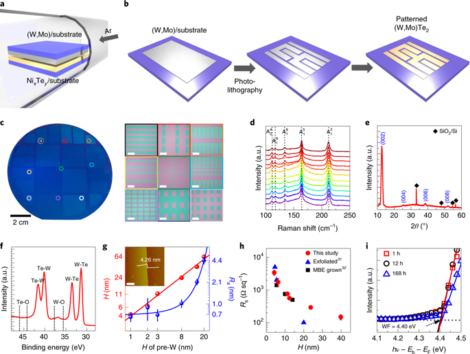
A key challenge in the development of two-dimensional (2D) devices is the fabrication of metal–semiconductor junctions with minimal contact resistance and depinned energy levels. An ideal solution for practical applications is to make contacts between 2D van der Waals semiconductors and 2D van der Waals metals. Here we report the wafer-scale production of patterned layers of metallic transition metal ditellurides on different substrates. Our tungsten ditelluride and molybdenum ditelluride layers, which are grown using a tellurization process applied to a precursor transition metal layer, have an electronic performance comparable to that of mechanically exfoliated flakes and can be combined with the 2D semiconductor molybdenum disulfide. The resulting metal–semiconductor junctions are free from significant disorder effects and Fermi-level pinning, and are used to create monolayer molybdenum disulfide field-effect transistors. The Schottky barrier heights of the devices also largely follow the trend of the Schottky–Mott limit.
中文翻译:
在肖特基-莫特极限条件下,用于二维金属-半导体接触的图案化过渡金属二碲化物层的晶圆级生产
二维(2D)器件开发中的关键挑战是制造具有最小接触电阻和固定能级的金属-半导体结。实际应用的理想解决方案是在2D范德华半导体和2D范德华金属之间建立接触。在这里,我们报告了在不同基板上的金属过渡金属二碲化物图案层的晶圆级生产。我们的二碲化钨和二碲化钼层是通过应用于前体过渡金属层的碲化工艺生长的,其电子性能可与机械剥离薄片媲美,并且可以与2D半导体二硫化钼结合使用。由此产生的金属-半导体结没有明显的无序效应和费米能级钉扎,并用于制造单层二硫化钼场效应晶体管。器件的肖特基势垒高度也很大程度上遵循了肖特基-莫特极限的趋势。


 京公网安备 11010802027423号