当前位置:
X-MOL 学术
›
Chem. Rev.
›
论文详情
Our official English website, www.x-mol.net, welcomes your feedback! (Note: you will need to create a separate account there.)
Wide Band Gap Chalcogenide Semiconductors.
Chemical Reviews ( IF 62.1 ) Pub Date : 2020-04-06 , DOI: 10.1021/acs.chemrev.9b00600 Rachel Woods-Robinson 1, 2, 3 , Yanbing Han 1, 4 , Hanyu Zhang 1 , Tursun Ablekim 1 , Imran Khan 1 , Kristin A Persson 3, 5 , Andriy Zakutayev 1
Chemical Reviews ( IF 62.1 ) Pub Date : 2020-04-06 , DOI: 10.1021/acs.chemrev.9b00600 Rachel Woods-Robinson 1, 2, 3 , Yanbing Han 1, 4 , Hanyu Zhang 1 , Tursun Ablekim 1 , Imran Khan 1 , Kristin A Persson 3, 5 , Andriy Zakutayev 1
Affiliation
|
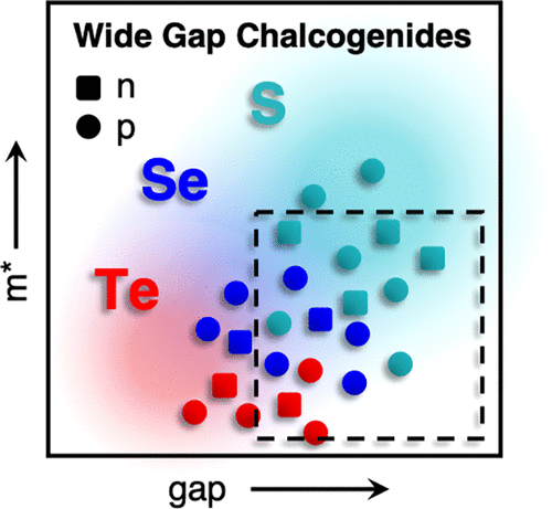
Wide band gap semiconductors are essential for today's electronic devices and energy applications because of their high optical transparency, controllable carrier concentration, and tunable electrical conductivity. The most intensively investigated wide band gap semiconductors are transparent conductive oxides (TCOs), such as tin-doped indium oxide (ITO) and amorphous In-Ga-Zn-O (IGZO), used in displays and solar cells, carbides (e.g., SiC) and nitrides (e.g., GaN) used in power electronics, and emerging halides (e.g., γ-CuI) and 2D electronic materials (e.g., graphene) used in various optoelectronic devices. Compared to these prominent materials families, chalcogen-based (Ch = S, Se, Te) wide band gap semiconductors are less heavily investigated but stand out because of their propensity for p-type doping, high mobilities, high valence band positions (i.e., low ionization potentials), and broad applications in electronic devices such as CdTe solar cells. This manuscript provides a review of wide band gap chalcogenide semiconductors. First, we outline general materials design parameters of high performing transparent semiconductors, as well as the theoretical and experimental underpinnings of the corresponding research methods. We proceed to summarize progress in wide band gap (EG > 2 eV) chalcogenide materials-namely, II-VI MCh binaries, CuMCh2 chalcopyrites, Cu3MCh4 sulvanites, mixed-anion layered CuMCh(O,F), and 2D materials-and discuss computational predictions of potential new candidates in this family, highlighting their optical and electrical properties. We finally review applications-for example, photovoltaic and photoelectrochemical solar cells, transistors, and light emitting diodes-that employ wide band gap chalcogenides as either an active or passive layer. By examining, categorizing, and discussing prospective directions in wide band gap chalcogenides, this Review aims to inspire continued research on this emerging class of transparent semiconductors and thereby enable future innovations for optoelectronic devices.
中文翻译:

宽带隙硫族化物半导体。
宽带隙半导体由于其高的光学透明度,可控制的载流子浓度和可调节的电导率,对于当今的电子设备和能源应用至关重要。研究最广泛的宽带隙半导体是透明导电氧化物(TCO),例如用于显示器和太阳能电池的掺锡氧化铟(ITO)和非晶In-Ga-Zn-O(IGZO),碳化物(例如电力电子中使用的SiC)和氮化物(例如GaN),以及各种光电设备中使用的新兴卤化物(例如γ-CuI)和2D电子材料(例如石墨烯)。与这些著名的材料系列相比,硫属元素(Ch = S,Se,Te)宽带隙半导体的研究较少,但由于它们倾向于p型掺杂,高迁移率,价带位置高(即低电离势),并在CdTe太阳能电池等电子设备中得到广泛应用。该手稿提供了宽带隙硫族化物半导体的综述。首先,我们概述了高性能透明半导体的一般材料设计参数,以及相应研究方法的理论和实验基础。我们继续总结宽带隙(EG> 2 eV)硫族化物材料的进展-即II-VI MCh二元,CuMCh2黄铜矿,Cu3MCh4亚硫酸盐,混合阴离子层状CuMCh(O,F)和2D材料-并讨论计算问题对这个家族中潜在的新候选人的预测,突出了他们的光学和电气特性。我们最终将审查应用程序,例如光伏和光电化学太阳能电池,晶体管和发光二极管-采用宽带隙硫族化物作为有源或无源层。通过审查,分类和讨论宽带隙硫族化物中的预期方向,本综述旨在激发对这一新兴类的透明半导体的持续研究,从而实现光电子器件的未来创新。
更新日期:2020-04-06
中文翻译:
宽带隙硫族化物半导体。
宽带隙半导体由于其高的光学透明度,可控制的载流子浓度和可调节的电导率,对于当今的电子设备和能源应用至关重要。研究最广泛的宽带隙半导体是透明导电氧化物(TCO),例如用于显示器和太阳能电池的掺锡氧化铟(ITO)和非晶In-Ga-Zn-O(IGZO),碳化物(例如电力电子中使用的SiC)和氮化物(例如GaN),以及各种光电设备中使用的新兴卤化物(例如γ-CuI)和2D电子材料(例如石墨烯)。与这些著名的材料系列相比,硫属元素(Ch = S,Se,Te)宽带隙半导体的研究较少,但由于它们倾向于p型掺杂,高迁移率,价带位置高(即低电离势),并在CdTe太阳能电池等电子设备中得到广泛应用。该手稿提供了宽带隙硫族化物半导体的综述。首先,我们概述了高性能透明半导体的一般材料设计参数,以及相应研究方法的理论和实验基础。我们继续总结宽带隙(EG> 2 eV)硫族化物材料的进展-即II-VI MCh二元,CuMCh2黄铜矿,Cu3MCh4亚硫酸盐,混合阴离子层状CuMCh(O,F)和2D材料-并讨论计算问题对这个家族中潜在的新候选人的预测,突出了他们的光学和电气特性。我们最终将审查应用程序,例如光伏和光电化学太阳能电池,晶体管和发光二极管-采用宽带隙硫族化物作为有源或无源层。通过审查,分类和讨论宽带隙硫族化物中的预期方向,本综述旨在激发对这一新兴类的透明半导体的持续研究,从而实现光电子器件的未来创新。


 京公网安备 11010802027423号