当前位置:
X-MOL 学术
›
Nano Lett.
›
论文详情
Our official English website, www.x-mol.net, welcomes your feedback! (Note: you will need to create a separate account there.)
Gate-Tunable Semiconductor Heterojunctions from 2D/3D van der Waals Interfaces
Nano Letters ( IF 10.8 ) Pub Date : 2020-03-20 , DOI: 10.1021/acs.nanolett.0c00741 Jinshui Miao 1 , Xiwen Liu 1 , Kiyoung Jo 1 , Kang He 2 , Ravindra Saxena 1 , Baokun Song 1 , Huiqin Zhang 1 , Jiale He 3 , Myung-Geun Han 4 , Weida Hu 3 , Deep Jariwala 1
Nano Letters ( IF 10.8 ) Pub Date : 2020-03-20 , DOI: 10.1021/acs.nanolett.0c00741 Jinshui Miao 1 , Xiwen Liu 1 , Kiyoung Jo 1 , Kang He 2 , Ravindra Saxena 1 , Baokun Song 1 , Huiqin Zhang 1 , Jiale He 3 , Myung-Geun Han 4 , Weida Hu 3 , Deep Jariwala 1
Affiliation
|
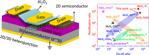
van der Waals (vdW) semiconductors are attractive for highly scaled devices and heterogeneous integration as they can be isolated into self-passivated, two-dimensional (2D) layers that enable superior electrostatic control. These attributes have led to numerous demonstrations of field-effect devices ranging from transistors to triodes. By exploiting the controlled, substitutional doping schemes in covalently bonded, three-dimensional (3D) semiconductors and the passivated surfaces of 2D semiconductors, one can construct devices that can exceed performance metrics of “all-2D” vdW heterojunctions. Here, we demonstrate 2D/3D semiconductor heterojunctions using MoS2 as the prototypical 2D semiconductor laid upon Si and GaN as the 3D semiconductor layers. By tuning the Fermi levels in MoS2, we demonstrate devices that concurrently exhibit over 7 orders of magnitude modulation in rectification ratios and conductance. Our results further suggest that the interface quality does not necessarily affect Fermi level tuning at the junction, opening up possibilities for novel 2D/3D heterojunction device architectures.
中文翻译:

来自2D / 3D van der Waals接口的栅极可调半导体异质结
范德华(vdW)半导体对于大规模器件和异质集成具有吸引力,因为它们可以隔离为能够进行出色静电控制的自钝化二维(2D)层。这些属性导致了从晶体管到三极管的众多场效应器件的演示。通过在共价键合的三维(3D)半导体和2D半导体的钝化表面中利用受控的替代掺杂方案,人们可以构建出性能指标超过“全2D” vdW异质结的器件。在这里,我们演示了使用MoS 2作为放置在Si和GaN上作为3D半导体层的原型2D半导体的2D / 3D半导体异质结。通过调整MoS 2中的费米能级,我们演示了在整流比和电导率上同时显示超过7个数量级调制的器件。我们的结果进一步表明,接口质量不一定会影响结处的费米能级调谐,从而为新颖的2D / 3D异质结器件体系结构开辟了可能性。
更新日期:2020-04-24
中文翻译:
来自2D / 3D van der Waals接口的栅极可调半导体异质结
范德华(vdW)半导体对于大规模器件和异质集成具有吸引力,因为它们可以隔离为能够进行出色静电控制的自钝化二维(2D)层。这些属性导致了从晶体管到三极管的众多场效应器件的演示。通过在共价键合的三维(3D)半导体和2D半导体的钝化表面中利用受控的替代掺杂方案,人们可以构建出性能指标超过“全2D” vdW异质结的器件。在这里,我们演示了使用MoS 2作为放置在Si和GaN上作为3D半导体层的原型2D半导体的2D / 3D半导体异质结。通过调整MoS 2中的费米能级,我们演示了在整流比和电导率上同时显示超过7个数量级调制的器件。我们的结果进一步表明,接口质量不一定会影响结处的费米能级调谐,从而为新颖的2D / 3D异质结器件体系结构开辟了可能性。


 京公网安备 11010802027423号