当前位置:
X-MOL 学术
›
Nanoscale Adv.
›
论文详情
Our official English website, www.x-mol.net, welcomes your feedback! (Note: you will need to create a separate account there.)
Synthesis of silicon carbide nanocrystals and multilayer graphitic carbon by femtosecond laser irradiation of polydimethylsiloxane
Nanoscale Advances ( IF 4.7 ) Pub Date : 2020-03-19 , DOI: 10.1039/d0na00133c Shuichiro Hayashi 1 , Fumiya Morosawa 2 , Mitsuhiro Terakawa 1, 2
Nanoscale Advances ( IF 4.7 ) Pub Date : 2020-03-19 , DOI: 10.1039/d0na00133c Shuichiro Hayashi 1 , Fumiya Morosawa 2 , Mitsuhiro Terakawa 1, 2
Affiliation
|
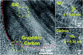
Laser-based modification of polymer materials has been emerging as a versatile and efficient technique to simultaneously form and pattern electrically conductive materials. Recently, it has been revealed that native polydimethylsiloxane (PDMS) can be modified into electrically conductive structures using femtosecond laser irradiation; however, the details regarding the structures formed by this method have yet to be revealed. In this work, structures were fabricated by focusing and scanning femtosecond laser pulses onto the surface of PDMS. Raman Spectroscopy and Transmission Electron Microscopy (TEM) analyses revealed the formation of silicon carbide (SiC) nanocrystals, as well as multilayer graphitic carbon, in the modified regions of PDMS. The state of the formed material differed depending on the distance from the focal spot, suggesting that photo-thermal effects contributed to the degradation of PDMS into conductive material. Electrical conductivity measurements, in addition to Raman results, indicated that the amount of disorder in the formed graphitic carbon contributes to the electrical conductivity of the fabricated structures.
中文翻译:

聚二甲基硅氧烷飞秒激光辐照合成碳化硅纳米晶和多层石墨碳
基于激光的聚合物材料改性已成为一种通用且有效的技术,可同时形成和图案化导电材料。最近,有研究表明,使用飞秒激光照射可以将天然聚二甲基硅氧烷 (PDMS) 改性为导电结构。然而,关于由这种方法形成的结构的细节尚未公布。在这项工作中,通过将飞秒激光脉冲聚焦和扫描到 PDMS 表面来制造结构。拉曼光谱和透射电子显微镜 (TEM) 分析揭示了在 PDMS 的改性区域中形成了碳化硅 (SiC) 纳米晶体以及多层石墨碳。成形材料的状态因距焦点的距离而异,表明光热效应有助于 PDMS 降解为导电材料。除了拉曼结果外,电导率测量表明,形成的石墨碳中的无序量有助于制造结构的电导率。
更新日期:2020-03-19
中文翻译:
聚二甲基硅氧烷飞秒激光辐照合成碳化硅纳米晶和多层石墨碳
基于激光的聚合物材料改性已成为一种通用且有效的技术,可同时形成和图案化导电材料。最近,有研究表明,使用飞秒激光照射可以将天然聚二甲基硅氧烷 (PDMS) 改性为导电结构。然而,关于由这种方法形成的结构的细节尚未公布。在这项工作中,通过将飞秒激光脉冲聚焦和扫描到 PDMS 表面来制造结构。拉曼光谱和透射电子显微镜 (TEM) 分析揭示了在 PDMS 的改性区域中形成了碳化硅 (SiC) 纳米晶体以及多层石墨碳。成形材料的状态因距焦点的距离而异,表明光热效应有助于 PDMS 降解为导电材料。除了拉曼结果外,电导率测量表明,形成的石墨碳中的无序量有助于制造结构的电导率。


 京公网安备 11010802027423号