当前位置:
X-MOL 学术
›
ACS Appl. Electron. Mater.
›
论文详情
Our official English website, www.x-mol.net, welcomes your feedback! (Note: you will need to create a separate account there.)
Transition from Hopping to Band-like Transport in Weakly Coupled Multilayer MoS2 Field Effect Transistors
ACS Applied Electronic Materials ( IF 4.7 ) Pub Date : 2020-03-13 , DOI: 10.1021/acsaelm.0c00046 Kailiang Huang 1, 2 , Miao Zhao 1, 2 , Bing Sun 1, 2 , Xueyuan Liu 1, 2 , Jianhua Liu 1, 2 , Hudong Chang 1, 2 , Yuping Zeng 3 , Honggang Liu 1, 2
ACS Applied Electronic Materials ( IF 4.7 ) Pub Date : 2020-03-13 , DOI: 10.1021/acsaelm.0c00046 Kailiang Huang 1, 2 , Miao Zhao 1, 2 , Bing Sun 1, 2 , Xueyuan Liu 1, 2 , Jianhua Liu 1, 2 , Hudong Chang 1, 2 , Yuping Zeng 3 , Honggang Liu 1, 2
Affiliation
|
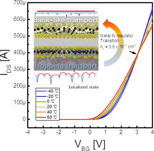
In this article, multilayer MoS2 manufactured from a multiple-transfer process of chemical vapor deposition (CVD)-grown monolayer MoS2 is studied. Because of the lattice mismatch and larger distance between adjacent MoS2 layers, the interlayer interaction is weakened and the band structure transition from direct to indirect as well as band gap shrinkage effect in multilayer is suppressed, as indicated by Raman and photoluminescence spectra. These structural differences from that of the exfoliated MoS2 make stacked MoS2 layers a better configuration for fabricating high-performance MoS2 field effect transistor (FET). Here, back-gate MoS2 FETs with different number of layers were fabricated. As the number of layers increases from 1 to 3, the devices’ mobility and on/off ratio show an enhancement from 2 to 62 cm2/s·V and 106 to 108, respectively. Metal-to-insulator transition (MIT) phenomena are also observed in bilayer MoS2 FET. A distributed resistance-based model is proposed to study the conductivity of weakly coupled MoS2 layers. Combining the resistance model with temperature dependence characteristics, it is demonstrated that the electron mobility in monolayer MoS2 is limited by the hopping transport mechanism, whereas the electron in the bilayer can be excited to band-like transport mode because of the immunity of the influence from the charge traps at the substrate, which explains the enhancement of mobility and MIT phenomena. This study is universally valid for other two-dimensional materials, paving way to fabricate high-performance nanoelectronics for integrated circuits.
中文翻译:

弱耦合多层MoS 2场效应晶体管中从跳变到带状传输的过渡
在本文中,研究了通过化学气相沉积(CVD)生长的单层MoS 2的多次转移工艺制造的多层MoS 2。由于晶格失配和相邻的MoS 2层之间的距离较大,层间的相互作用被削弱,并且从直接到间接的能带结构转变以及多层中的带隙收缩效应受到抑制,如拉曼光谱和光致发光光谱所示。这些与剥离的MoS 2的结构差异使堆叠的MoS 2层成为制造高性能MoS 2场效应晶体管(FET)的更好配置。在这里,背栅MoS 2制作了具有不同层数的FET。随着层数从1增加到3,设备的迁移率和开/关比分别从2到62 cm 2 / s·V和10 6到10 8增强。在双层MoS 2 FET中也观察到金属到绝缘体的转变(MIT)现象。提出了一种基于分布电阻的模型来研究弱耦合MoS 2层的电导率。结合电阻模型和温度依赖性特性,证明了单层MoS 2中的电子迁移率受跳变传输机制的限制,而双层中的电子却可以被激发成带状传输模式,这是因为不受衬底电荷陷阱的影响,这解释了迁移率和MIT现象的增强。这项研究对其他二维材料普遍有效,为制造集成电路的高性能纳米电子学铺平了道路。
更新日期:2020-03-13
中文翻译:
弱耦合多层MoS 2场效应晶体管中从跳变到带状传输的过渡
在本文中,研究了通过化学气相沉积(CVD)生长的单层MoS 2的多次转移工艺制造的多层MoS 2。由于晶格失配和相邻的MoS 2层之间的距离较大,层间的相互作用被削弱,并且从直接到间接的能带结构转变以及多层中的带隙收缩效应受到抑制,如拉曼光谱和光致发光光谱所示。这些与剥离的MoS 2的结构差异使堆叠的MoS 2层成为制造高性能MoS 2场效应晶体管(FET)的更好配置。在这里,背栅MoS 2制作了具有不同层数的FET。随着层数从1增加到3,设备的迁移率和开/关比分别从2到62 cm 2 / s·V和10 6到10 8增强。在双层MoS 2 FET中也观察到金属到绝缘体的转变(MIT)现象。提出了一种基于分布电阻的模型来研究弱耦合MoS 2层的电导率。结合电阻模型和温度依赖性特性,证明了单层MoS 2中的电子迁移率受跳变传输机制的限制,而双层中的电子却可以被激发成带状传输模式,这是因为不受衬底电荷陷阱的影响,这解释了迁移率和MIT现象的增强。这项研究对其他二维材料普遍有效,为制造集成电路的高性能纳米电子学铺平了道路。


 京公网安备 11010802027423号