Nature Materials ( IF 41.2 ) Pub Date : 2020-03-09 , DOI: 10.1038/s41563-020-0636-5 Xuezeng Tian 1 , Dennis S Kim 1 , Shize Yang 2, 3 , Christopher J Ciccarino 4, 5 , Yongji Gong 6 , Yongsoo Yang 1, 7 , Yao Yang 1 , Blake Duschatko 4 , Yakun Yuan 1 , Pulickel M Ajayan 6 , Juan Carlos Idrobo 2 , Prineha Narang 4 , Jianwei Miao 1
|
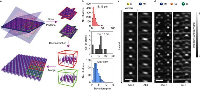
The electronic, optical and chemical properties of two-dimensional transition metal dichalcogenides strongly depend on their three-dimensional atomic structure and crystal defects. Using Re-doped MoS2 as a model system, here we present scanning atomic electron tomography as a method to determine three-dimensional atomic positions as well as positions of crystal defects such as dopants, vacancies and ripples with a precision down to 4 pm. We measure the three-dimensional bond distortion and local strain tensor induced by single dopants. By directly providing these experimental three-dimensional atomic coordinates to density functional theory, we obtain more accurate electronic band structures than derived from conventional density functional theory calculations that relies on relaxed three-dimensional atomic coordinates. We anticipate that scanning atomic electron tomography not only will be generally applicable to determine the three-dimensional atomic coordinates of two-dimensional materials, but also will enable ab initio calculations to better predict the physical, chemical and electronic properties of these materials.
中文翻译:
关联二维过渡金属二卤化物的三维原子缺陷和电子性质。
二维过渡金属二卤化物的电子,光学和化学性质在很大程度上取决于其三维原子结构和晶体缺陷。使用重掺杂的MoS 2作为模型系统,在这里,我们介绍扫描原子电子断层扫描技术,该方法可确定三维原子位置以及晶体缺陷(例如掺杂剂,空位和波纹)的位置,精度可低至4 pm。我们测量了由单一掺杂剂引起的三维键变形和局部应变张量。通过将这些实验性的三维原子坐标直接提供给密度泛函理论,我们得到的电子能带结构比依赖于轻松的三维原子坐标的传统密度泛函理论计算得出的电子带结构更为精确。我们预计,扫描原子电子断层扫描不仅将普遍适用于确定二维材料的三维原子坐标,


 京公网安备 11010802027423号