当前位置:
X-MOL 学术
›
ACS Appl. Electron. Mater.
›
论文详情
Our official English website, www.x-mol.net, welcomes your feedback! (Note: you will need to create a separate account there.)
Assembly, Stability, and Electrical Properties of Sparse Crystalline Silicon Nanoparticle Networks Applied to Solution-Processed Field-Effect Transistors
ACS Applied Electronic Materials ( IF 4.7 ) Pub Date : 2020-02-20 , DOI: 10.1021/acsaelm.9b00786 Domenikos Chryssikos 1 , Markus Wiesinger 1 , Oliver Bienek 1 , Hartmut Wiggers 2 , Martin Stutzmann 1 , Anna Cattani-Scholz 1 , Rui N. Pereira 1, 3
ACS Applied Electronic Materials ( IF 4.7 ) Pub Date : 2020-02-20 , DOI: 10.1021/acsaelm.9b00786 Domenikos Chryssikos 1 , Markus Wiesinger 1 , Oliver Bienek 1 , Hartmut Wiggers 2 , Martin Stutzmann 1 , Anna Cattani-Scholz 1 , Rui N. Pereira 1, 3
Affiliation
|
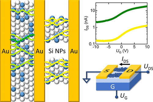
Thin films of crystalline silicon nanoparticles (Si NPs) processed from liquid dispersions of NPs (NP inks) using printing-type deposition methods are currently being intensively investigated for the development of electronic and optoelectronic nanotechnologies. Various (opto)electronic applications have already been demonstrated based on these materials, but so far, devices exhibit modest performance because of relatively low electrical conductivity and charge carrier mobility. In this work, we aim at unveiling the major factors affecting the long-range transport of charges in Si NP thin films. For this, we monitor the electrical properties of thin-film field effect transistors (FETs) as the active channel of the devices is gradually filled with Si NPs. To produce these FET devices featuring stable, sparse Si NP networks within the active channel, we developed a fabrication protocol based on NP deposition by device substrate immersion in a NP ink, made of Si NPs and chlorobenzene, followed by annealing and ultrasonication. We found that both the electrical conductivity and the charge carrier mobility of the FETs increase extremely rapidly as the device channel coverage with NPs increases. Thus, the NP network corresponds effectively to an inhomogeneous blend of conducting and insulating Si NPs, with the most efficient charge percolation paths involving only a fraction of the NPs. We discuss the factors that may lead to this behavior, in view of developing Si NP thin films with competitive charge transport characteristics.
中文翻译:

稀疏晶体硅纳米粒子网络的组装,稳定性和电性能,应用于溶液处理的场效应晶体管
目前正在深入研究使用印刷型沉积方法从NPs(NP墨水)的液体分散体加工而成的晶体硅纳米颗粒(Si NPs)的薄膜,以发展电子和光电子纳米技术。基于这些材料已经证明了各种(光电)电子应用,但是到目前为止,由于相对较低的电导率和电荷载流子迁移率,设备表现出适度的性能。在这项工作中,我们旨在揭示影响Si NP薄膜中电荷的长距离传输的主要因素。为此,当器件的有源通道逐渐被Si NP填充时,我们监视薄膜场效应晶体管(FET)的电性能。为了生产在有源通道内具有稳定,稀疏Si NP网络的FET器件,我们开发了一种基于NP沉积的制造方案,该方案通过将器件基板浸入由NP和氯苯制成的NP墨水中,然后进行退火和超声处理来实现。我们发现,随着NPs的器件通道覆盖率的增加,FET的电导率和电荷载流子迁移率都迅速增加。因此,NP网络有效地对应于导电和绝缘Si NP的不均匀混合,其中最有效的电荷渗透路径仅涉及一部分NP。鉴于开发具有竞争性电荷传输特性的Si NP薄膜,我们讨论了可能导致这种行为的因素。然后进行退火和超声处理。我们发现,随着NPs的器件通道覆盖率的增加,FET的电导率和电荷载流子迁移率都迅速增加。因此,NP网络有效地对应于导电和绝缘Si NP的不均匀混合,其中最有效的电荷渗透路径仅涉及一部分NP。考虑到开发具有竞争性电荷传输特性的Si NP薄膜,我们讨论了可能导致这种行为的因素。然后进行退火和超声处理。我们发现,随着NPs的器件通道覆盖率的增加,FET的电导率和电荷载流子迁移率都迅速增加。因此,NP网络有效地对应于导电和绝缘Si NP的不均匀混合,其中最有效的电荷渗透路径仅涉及一部分NP。鉴于开发具有竞争性电荷传输特性的Si NP薄膜,我们讨论了可能导致这种行为的因素。最有效的电荷渗透路径仅涉及一部分NP。鉴于开发具有竞争性电荷传输特性的Si NP薄膜,我们讨论了可能导致这种行为的因素。最有效的电荷渗透路径仅涉及一部分NP。鉴于开发具有竞争性电荷传输特性的Si NP薄膜,我们讨论了可能导致这种行为的因素。
更新日期:2020-02-20
中文翻译:
稀疏晶体硅纳米粒子网络的组装,稳定性和电性能,应用于溶液处理的场效应晶体管
目前正在深入研究使用印刷型沉积方法从NPs(NP墨水)的液体分散体加工而成的晶体硅纳米颗粒(Si NPs)的薄膜,以发展电子和光电子纳米技术。基于这些材料已经证明了各种(光电)电子应用,但是到目前为止,由于相对较低的电导率和电荷载流子迁移率,设备表现出适度的性能。在这项工作中,我们旨在揭示影响Si NP薄膜中电荷的长距离传输的主要因素。为此,当器件的有源通道逐渐被Si NP填充时,我们监视薄膜场效应晶体管(FET)的电性能。为了生产在有源通道内具有稳定,稀疏Si NP网络的FET器件,我们开发了一种基于NP沉积的制造方案,该方案通过将器件基板浸入由NP和氯苯制成的NP墨水中,然后进行退火和超声处理来实现。我们发现,随着NPs的器件通道覆盖率的增加,FET的电导率和电荷载流子迁移率都迅速增加。因此,NP网络有效地对应于导电和绝缘Si NP的不均匀混合,其中最有效的电荷渗透路径仅涉及一部分NP。鉴于开发具有竞争性电荷传输特性的Si NP薄膜,我们讨论了可能导致这种行为的因素。然后进行退火和超声处理。我们发现,随着NPs的器件通道覆盖率的增加,FET的电导率和电荷载流子迁移率都迅速增加。因此,NP网络有效地对应于导电和绝缘Si NP的不均匀混合,其中最有效的电荷渗透路径仅涉及一部分NP。考虑到开发具有竞争性电荷传输特性的Si NP薄膜,我们讨论了可能导致这种行为的因素。然后进行退火和超声处理。我们发现,随着NPs的器件通道覆盖率的增加,FET的电导率和电荷载流子迁移率都迅速增加。因此,NP网络有效地对应于导电和绝缘Si NP的不均匀混合,其中最有效的电荷渗透路径仅涉及一部分NP。鉴于开发具有竞争性电荷传输特性的Si NP薄膜,我们讨论了可能导致这种行为的因素。最有效的电荷渗透路径仅涉及一部分NP。鉴于开发具有竞争性电荷传输特性的Si NP薄膜,我们讨论了可能导致这种行为的因素。最有效的电荷渗透路径仅涉及一部分NP。鉴于开发具有竞争性电荷传输特性的Si NP薄膜,我们讨论了可能导致这种行为的因素。


 京公网安备 11010802027423号