当前位置:
X-MOL 学术
›
Opt. Lett.
›
论文详情
Our official English website, www.x-mol.net, welcomes your feedback! (Note: you will need to create a separate account there.)
Silicon-based high-responsivity GeSn short-wave infrared heterojunction phototransistors with a floating base.
Optics Letters ( IF 3.6 ) Pub Date : 2020-03-01 , DOI: 10.1364/ol.383171 Wei-Ting Hung , Devesh Barshilia , Rikmantra Basu , H. H. Cheng , Guo-En Chang
Optics Letters ( IF 3.6 ) Pub Date : 2020-03-01 , DOI: 10.1364/ol.383171 Wei-Ting Hung , Devesh Barshilia , Rikmantra Basu , H. H. Cheng , Guo-En Chang
|
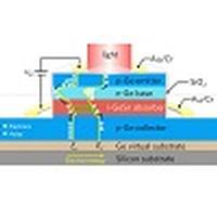
We demonstrate silicon-based $p \text{-} n \text{-} p$p-n-p floating-base GeSn heterojunction phototransistors with enhanced optical responsivity for efficient short-wave infrared (SWIR) photodetection. The narrow-bandgap GeSn active layer sandwiched between the $p \text{-} {\rm Ge}$p-Ge collector and $n \text{-} {\rm Ge}$n-Ge base effectively extends the photodetection range in the SWIR range, and the internal gain amplifies the optical response by a factor of more than three at a low driving voltage of 0.4 V compared to that of a reference GeSn $p \text{-} i \text{-} n$p-i-n photodetector (PD). We anticipate that our findings will be leveraged to realize complementary metal-oxide-semiconductor-compatible, sensitive, low driving voltage SWIR PDs in a wide range of applications.
中文翻译:

具有浮动基极的硅基高响应GeSn短波红外异质结光电晶体管。
我们演示了基于硅的$ p \ text {-} n \ text {-} p $ pnp浮基GeSn异质结光电晶体管,该晶体管具有增强的光学响应能力,可用于有效的短波红外(SWIR)光检测。夹在$ p \ text {-} {\ rm Ge} $ p-Ge集电极和$ n \ text {-} {\ rm Ge} $ n-Ge基极之间的窄带隙GeSn有源层有效地扩展了光检测范围与参考GeSn $ p \ text {-} i \ text {-} n $相比,内部增益在0.4 V的低驱动电压下将光学响应放大三倍以上。引脚光电探测器(PD)。我们预计,我们的发现将被用于实现与金属氧化物半导体兼容的互补型,灵敏的,低驱动电压的SWIR PD,广泛应用于各种应用中。
更新日期:2020-02-28
中文翻译:
具有浮动基极的硅基高响应GeSn短波红外异质结光电晶体管。
我们演示了基于硅的$ p \ text {-} n \ text {-} p $ pnp浮基GeSn异质结光电晶体管,该晶体管具有增强的光学响应能力,可用于有效的短波红外(SWIR)光检测。夹在$ p \ text {-} {\ rm Ge} $ p-Ge集电极和$ n \ text {-} {\ rm Ge} $ n-Ge基极之间的窄带隙GeSn有源层有效地扩展了光检测范围与参考GeSn $ p \ text {-} i \ text {-} n $相比,内部增益在0.4 V的低驱动电压下将光学响应放大三倍以上。引脚光电探测器(PD)。我们预计,我们的发现将被用于实现与金属氧化物半导体兼容的互补型,灵敏的,低驱动电压的SWIR PD,广泛应用于各种应用中。


 京公网安备 11010802027423号