当前位置:
X-MOL 学术
›
Adv. Mater.
›
论文详情
Our official English website, www.x-mol.net, welcomes your feedback! (Note: you will need to create a separate account there.)
Enhanced Vertical Charge Transport of Homo- and Blended Semiconducting Polymers by Nanoconfinement.
Advanced Materials ( IF 29.4 ) Pub Date : 2020-01-27 , DOI: 10.1002/adma.201908087 Jongkuk Ko 1 , Youngkeol Kim 1 , Jin Soo Kang 2 , Rüdiger Berger 3 , Hyunsik Yoon 4 , Kookheon Char 1
Advanced Materials ( IF 29.4 ) Pub Date : 2020-01-27 , DOI: 10.1002/adma.201908087 Jongkuk Ko 1 , Youngkeol Kim 1 , Jin Soo Kang 2 , Rüdiger Berger 3 , Hyunsik Yoon 4 , Kookheon Char 1
Affiliation
|
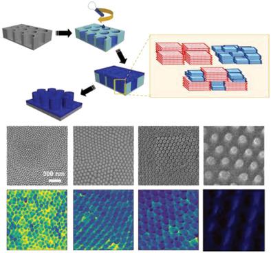
The morphology of conjugated polymers has critical influences on electronic and optical properties of optoelectronic devices. Even though lots of techniques and methods are suggested to control the morphology of polymers, very few studies have been performed inducing high charge transport along out-of-plane direction. In this study, the self-assembly of homo- and blended conjugated polymers which are confined in nanostructures is utilized. The resulting structures lead to high charge mobility along vertical direction for both homo- and blended conjugated polymers. Both semicrystalline and amorphous polymers show highly increased population of face-on crystallite despite intrinsic crystallinity of polymers. They result in more than two orders of magnitude enhanced charge mobility along vertical direction revealed by nanoscale conductive scanning force microscopy and macroscale IV characteristic measurements. Moreover, blends of semicrystalline and amorphous polymers, which are known to show inferior optical and electrical properties due to their structural incompatibility, are formed into harmonious states by this approach. Assembly of blends of semicrystalline and amorphous polymers under nanoconfinement shows charge mobility in out-of-plane direction of 0.73 cm2 V-1 s-1 with wide range of absorption wavelength from 300 to 750 nm demonstrating the synergistic effects of two different polymers.
中文翻译:

通过纳米约束增强了均聚物和共混半导体聚合物的垂直电荷传输。
共轭聚合物的形态对光电器件的电子和光学性能有关键影响。尽管提出了许多控制聚合物形态的技术和方法,但很少有研究引起沿平面外方向的高电荷传输。在这项研究中,利用了均聚物和共混聚合物的自组装,它们被限制在纳米结构中。对于均聚和共混的共轭聚合物,所得结构均导致沿垂直方向的高电荷迁移率。尽管聚合物具有固有的结晶性,但半结晶和无定形聚合物都显示出大量增加的面对微晶。它们导致纳米级导电扫描力显微镜和宏观IV特性测量揭示的沿垂直方向的电荷迁移率提高了两个数量级以上。此外,通过这种方法将已知由于其结构不相容而显示出较差的光学和电性能的半结晶和无定形聚合物的共混物形成和谐状态。纳米约束下的半结晶和非晶态聚合物共混物的组装显示,其面外方向的电荷迁移率为0.73 cm2 V-1 s-1,吸收波长范围为300至750 nm,这表明了两种不同聚合物的协同效应。由于它们的结构不相容性而已知显示出较差的光学和电学性质的化合物,通过这种方法被形成为和谐状态。纳米约束下的半结晶和非晶态聚合物共混物的组装显示,其面外方向的电荷迁移率为0.73 cm2 V-1 s-1,吸收波长范围为300至750 nm,这表明了两种不同聚合物的协同效应。由于它们的结构不相容性而已知显示出较差的光学和电学性质的化合物,通过这种方法被形成为和谐状态。纳米约束下的半结晶和非晶态聚合物共混物的组装显示,其面外方向的电荷迁移率为0.73 cm2 V-1 s-1,吸收波长范围为300至750 nm,这表明了两种不同聚合物的协同效应。
更新日期:2020-03-09
中文翻译:
通过纳米约束增强了均聚物和共混半导体聚合物的垂直电荷传输。
共轭聚合物的形态对光电器件的电子和光学性能有关键影响。尽管提出了许多控制聚合物形态的技术和方法,但很少有研究引起沿平面外方向的高电荷传输。在这项研究中,利用了均聚物和共混聚合物的自组装,它们被限制在纳米结构中。对于均聚和共混的共轭聚合物,所得结构均导致沿垂直方向的高电荷迁移率。尽管聚合物具有固有的结晶性,但半结晶和无定形聚合物都显示出大量增加的面对微晶。它们导致纳米级导电扫描力显微镜和宏观IV特性测量揭示的沿垂直方向的电荷迁移率提高了两个数量级以上。此外,通过这种方法将已知由于其结构不相容而显示出较差的光学和电性能的半结晶和无定形聚合物的共混物形成和谐状态。纳米约束下的半结晶和非晶态聚合物共混物的组装显示,其面外方向的电荷迁移率为0.73 cm2 V-1 s-1,吸收波长范围为300至750 nm,这表明了两种不同聚合物的协同效应。由于它们的结构不相容性而已知显示出较差的光学和电学性质的化合物,通过这种方法被形成为和谐状态。纳米约束下的半结晶和非晶态聚合物共混物的组装显示,其面外方向的电荷迁移率为0.73 cm2 V-1 s-1,吸收波长范围为300至750 nm,这表明了两种不同聚合物的协同效应。由于它们的结构不相容性而已知显示出较差的光学和电学性质的化合物,通过这种方法被形成为和谐状态。纳米约束下的半结晶和非晶态聚合物共混物的组装显示,其面外方向的电荷迁移率为0.73 cm2 V-1 s-1,吸收波长范围为300至750 nm,这表明了两种不同聚合物的协同效应。


 京公网安备 11010802027423号