Communications Physics ( IF 5.5 ) Pub Date : 2020-01-21 , DOI: 10.1038/s42005-020-0290-x Zakhar R. Kudrynskyi , James Kerfoot , Debarati Mazumder , Mark T. Greenaway , Evgeni E. Vdovin , Oleg Makarovsky , Zakhar D. Kovalyuk , Laurence Eaves , Peter H. Beton , Amalia Patanè
|
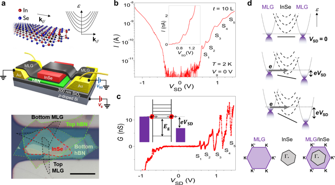
Two-dimensional (2D) van der Waals (vdW) crystals have attracted considerable interest for digital electronics beyond Si-based complementary metal oxide semiconductor technologies. Despite the transformative success of Si-based devices, there are limits to their miniaturization and functionalities. Here we realize a resonant tunnelling transistor (RTT) based on a 2D InSe layer sandwiched between two multilayered graphene (MLG) electrodes. In the RTT the energy of the quantum-confined 2D subbands of InSe can be tuned by the thickness of the InSe layer. By applying a voltage across the two MLG electrodes, which serve as the source and drain electrodes to the InSe, the chemical potential in the source can be tuned in and out of resonance with a given 2D subband, leading to multiple regions of negative differential conductance that can be additionally tuned by electrostatic gating. This work demonstrates the potential of InSe and InSe-based RTTs for applications in quantum electronics.
中文翻译:
共振隧穿到InSe层的二维子带中
二维(2D)范德华(vdW)晶体引起了数字电子领域的广泛关注,而硅基互补金属氧化物半导体技术除外。尽管基于Si的设备取得了巨大的成功,但是它们的小型化和功能仍然受到限制。在这里,我们实现了一个基于2D InSe层的谐振隧穿晶体管(RTT),该层夹在两个多层石墨烯(MLG)电极之间。在RTT中,可以通过InSe层的厚度来调整InSe的量子限制2D子带的能量。通过在用作InSe的源电极和漏电极的两个MLG电极之间施加电压,可以在给定的2D子带中调节源中的化学势,使之处于和不处于共振状态,导致负差分电导的多个区域,可以通过静电门控对其进行额外调整。这项工作证明了InSe和基于InSe的RTT在量子电子学中的应用潜力。


 京公网安备 11010802027423号