当前位置:
X-MOL 学术
›
Adv. Mater.
›
论文详情
Our official English website, www.x-mol.net, welcomes your feedback! (Note: you will need to create a separate account there.)
Lateral 2D WSe2 p-n Homojunction Formed by Efficient Charge-Carrier-Type Modulation for High-Performance Optoelectronics.
Advanced Materials ( IF 29.4 ) Pub Date : 2020-01-20 , DOI: 10.1002/adma.201906499 Jiacheng Sun 1 , Yuyan Wang 1 , Shaoqiang Guo 1 , Bensong Wan 2 , Lianqing Dong 1 , Youdi Gu 3 , Cheng Song 3 , Caofeng Pan 2 , Qinghua Zhang 4 , Lin Gu 4 , Feng Pan 3 , Junying Zhang 1
Advanced Materials ( IF 29.4 ) Pub Date : 2020-01-20 , DOI: 10.1002/adma.201906499 Jiacheng Sun 1 , Yuyan Wang 1 , Shaoqiang Guo 1 , Bensong Wan 2 , Lianqing Dong 1 , Youdi Gu 3 , Cheng Song 3 , Caofeng Pan 2 , Qinghua Zhang 4 , Lin Gu 4 , Feng Pan 3 , Junying Zhang 1
Affiliation
|
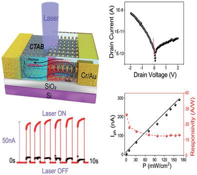
As unique building blocks for next-generation optoelectronics, high-quality 2D p-n junctions based on semiconducting transition metal dichalcogenides (TMDs) have attracted wide interest, which are urgent to be exploited. Herein, a novel and facile electron doping of WSe2 by cetyltrimethyl ammonium bromide (CTAB) is achieved for the first time to form a high-quality intramolecular p-n junction with superior optoelectronic properties. Efficient manipulation of charge carrier type and density in TMDs via electron transfer between Br- in CTAB and TMDs is proposed theoretically by density functional theory (DFT) calculations. Compared with the intrinsic WSe2 photodetector, the switching light ratio (Ilight /Idark ) of the p-n junction device can be enhanced by 103 , and the temporal response is also dramatically improved. The device possesses a responsivity of 30 A W-1 , with a specific detectivity of over 1011 Jones. In addition, the mechanism of charge transfer in CTAB-doped 2D WSe2 and WS2 are investigated by designing high-performance field effect transistors. Besides the scientific insight into the effective manipulation of 2D materials by chemical doping, this work presents a promising applicable approach toward next-generation photoelectronic devices with high efficiency.
中文翻译:

横向2D WSe2 pn同质结由高性能光电器件的有效电荷载流子类型调制形成。
作为下一代光电子学的独特构建基块,基于半导体过渡金属二卤化金属(TMD)的高质量2D pn结引起了广泛的兴趣,迫在眉睫。本文中,首次实现了十六烷基三甲基溴化铵(CTAB)对WSe2的新颖,便捷的电子掺杂,以形成具有优异光电性能的高质量分子内pn结。通过密度泛函理论(DFT)计算从理论上提出了通过CTAB中的Br-与TMDs之间的电子转移来有效控制TMDs中载流子类型和密度的方法。与本征WSe2光电探测器相比,pn结器件的开关光比(Ilight / Idark)可以提高103,并且时间响应也得到显着改善。该设备具有30 A W-1的响应度,比检测率超过1011 Jones。此外,通过设计高性能的场效应晶体管,研究了掺杂CTAB的2D WSe2和WS2中电荷转移的机理。除了对化学掺杂对2D材料进行有效处理的科学见解之外,这项工作还为高效率的下一代光电器件提供了一种有前途的可应用方法。
更新日期:2020-03-03
中文翻译:
横向2D WSe2 pn同质结由高性能光电器件的有效电荷载流子类型调制形成。
作为下一代光电子学的独特构建基块,基于半导体过渡金属二卤化金属(TMD)的高质量2D pn结引起了广泛的兴趣,迫在眉睫。本文中,首次实现了十六烷基三甲基溴化铵(CTAB)对WSe2的新颖,便捷的电子掺杂,以形成具有优异光电性能的高质量分子内pn结。通过密度泛函理论(DFT)计算从理论上提出了通过CTAB中的Br-与TMDs之间的电子转移来有效控制TMDs中载流子类型和密度的方法。与本征WSe2光电探测器相比,pn结器件的开关光比(Ilight / Idark)可以提高103,并且时间响应也得到显着改善。该设备具有30 A W-1的响应度,比检测率超过1011 Jones。此外,通过设计高性能的场效应晶体管,研究了掺杂CTAB的2D WSe2和WS2中电荷转移的机理。除了对化学掺杂对2D材料进行有效处理的科学见解之外,这项工作还为高效率的下一代光电器件提供了一种有前途的可应用方法。


 京公网安备 11010802027423号