Our official English website, www.x-mol.net, welcomes your feedback! (Note: you will need to create a separate account there.)
Low-Power Switching through Disorder and Carrier Localization in Bismuth-Doped Germanium Telluride Phase Change Memory Nanowires.
ACS Nano ( IF 17.1 ) Pub Date : 2020-01-23 , DOI: 10.1021/acsnano.9b08986 Gaurav Modi 1 , Eric A Stach 1 , Ritesh Agarwal 1
ACS Nano ( IF 17.1 ) Pub Date : 2020-01-23 , DOI: 10.1021/acsnano.9b08986 Gaurav Modi 1 , Eric A Stach 1 , Ritesh Agarwal 1
Affiliation
|
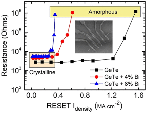
One of the major problems with phase change memory (PCM) is the high current density required for the crystal-amorphous transformation via a melt-quench process. However, alternative low-energy pathways of amorphization via a defect-assisted process have also been proposed. Here, a defect-assisted amorphization pathway in Bi-doped GeTe nanowires is utilized to establish that carrier localization effects can significantly decrease the energy costs of amorphization. We demonstrate a strategy of doping GeTe nanowires with bismuth to engineer carrier localization effects via Fermi level/mobility edge tuning and increased atomic disorder. Enhanced carrier localization increases the carrier-lattice coupling, and therefore, the energy supplied to carriers via electrical pulses can be more efficiently extracted by the lattice to induce the critical bond distortions required for amorphization without an intermediate melting process. RESET (crystal to amorphous transition) current densities as low as ∼0.3 MA cm-2 are achieved for 8% Bi-doped GeTe nanowires, which is nearly a 3-fold reduction compared to undoped GeTe nanowires and is significantly less than GeTe thin film devices (∼50 MA cm-2). We demonstrate good reversibility of switching in the Bi-doped GeTe nanowires and also demonstrate the existence of intermediate resistance states which can be accessed by controlled electrical pulsing. The combination of low-power switching in conjunction with multiple resistance states indicates that doping strategies in PCM nanowires are beneficial for non-volatile memory and neuromorphic computing applications.
中文翻译:

铋掺杂碲化锗相变存储纳米线中无序和载流子定位的低功率开关。
相变存储器(PCM)的主要问题之一是通过熔体淬火过程进行晶体非晶转变所需的高电流密度。但是,还提出了通过缺陷辅助工艺进行非晶化的其他低能途径。在这里,利用Bi掺杂GeTe纳米线中的缺陷辅助非晶化途径来建立载流子定位效应可以显着降低非晶化的能量成本。我们展示了用铋掺杂GeTe纳米线以通过费米能级/迁移率边缘调整和增加的原子无序来设计载流子定位效应的策略。增强的载流子定位可增加载流子-晶格耦合,因此,晶格可以更有效地提取通过电脉冲提供给载流子的能量,从而在不经过中间熔化过程的情况下诱发非晶化所需的临界键变形。8%的Bi掺杂GeTe纳米线可实现低至约0.3 MA cm-2的RESET(晶体到非晶态转变)电流密度,与未掺杂的GeTe纳米线相比,该电流密度降低了近三倍,并且显着低于GeTe薄膜装置(〜50 MA cm-2)。我们展示了Bi掺杂的GeTe纳米线中开关的良好可逆性,还展示了可通过受控电脉冲访问的中间电阻状态的存在。
更新日期:2020-01-23
中文翻译:
铋掺杂碲化锗相变存储纳米线中无序和载流子定位的低功率开关。
相变存储器(PCM)的主要问题之一是通过熔体淬火过程进行晶体非晶转变所需的高电流密度。但是,还提出了通过缺陷辅助工艺进行非晶化的其他低能途径。在这里,利用Bi掺杂GeTe纳米线中的缺陷辅助非晶化途径来建立载流子定位效应可以显着降低非晶化的能量成本。我们展示了用铋掺杂GeTe纳米线以通过费米能级/迁移率边缘调整和增加的原子无序来设计载流子定位效应的策略。增强的载流子定位可增加载流子-晶格耦合,因此,晶格可以更有效地提取通过电脉冲提供给载流子的能量,从而在不经过中间熔化过程的情况下诱发非晶化所需的临界键变形。8%的Bi掺杂GeTe纳米线可实现低至约0.3 MA cm-2的RESET(晶体到非晶态转变)电流密度,与未掺杂的GeTe纳米线相比,该电流密度降低了近三倍,并且显着低于GeTe薄膜装置(〜50 MA cm-2)。我们展示了Bi掺杂的GeTe纳米线中开关的良好可逆性,还展示了可通过受控电脉冲访问的中间电阻状态的存在。


 京公网安备 11010802027423号