当前位置:
X-MOL 学术
›
Appl. Surf. Sci.
›
论文详情
Our official English website, www.x-mol.net, welcomes your feedback! (Note: you will need to create a separate account there.)
Improvement of Ti/Al Ohmic Contacts on N-face n-type GaN by using O2 Plasma Treatment
Applied Surface Science ( IF 6.7 ) Pub Date : 2020-04-01 , DOI: 10.1016/j.apsusc.2019.145180 Hyeuk Seo , Yu-Jung Cha , Abu Bashar Mohammad Hamidul Islam , Joon Seop Kwak
Applied Surface Science ( IF 6.7 ) Pub Date : 2020-04-01 , DOI: 10.1016/j.apsusc.2019.145180 Hyeuk Seo , Yu-Jung Cha , Abu Bashar Mohammad Hamidul Islam , Joon Seop Kwak
|
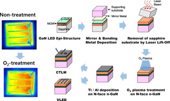
Abstract The effect of O2 plasma treatment on the electrical properties of Ti/Al (20/200 nm) contact to N (Nitrogen)-face n-GaN of vertical light-emitting diodes (VLEDs) has been investigated by varying the O2 plasma treatment power and time. Both photolithography and chemical lift-off methods are used to prepare the circular transfer length method (CTLM) patterns on the N-face n-GaN for measuring the contact and sheet resistances. Both total and sheet resistances are decreased with the increase in plasma treatment power up to 250 W. It is found that the Ti/Al-based Schottky contact layer transforms to ohmic characteristics after plasma treatment. Ga N chemical bonds on the n-GaN surface are broken due to O2 plasma treatment; thus, resulting in formed Ga O bonds which are interactively understood by using X-ray photoelectron spectroscopy characteristics. After plasma treatment, the forward voltage of VLED is not only reduced owing to decrease in total resistance but also both the light intensity distribution and the light-output-power are improved because of increase in current spreading through the contact layer.
中文翻译:

使用 O2 等离子体处理改进 N 面 n 型 GaN 上的 Ti/Al 欧姆接触
摘要 通过改变 O2 等离子体处理,研究了 O2 等离子体处理对垂直发光二极管 (VLED) 的 N(氮)面 n-GaN 接触的 Ti/Al(20/200 nm)电性能的影响。权力和时间。光刻和化学剥离方法都用于在 N 面 n-GaN 上制备圆形转移长度法 (CTLM) 图案,用于测量接触电阻和薄层电阻。随着等离子体处理功率增加到 250 W,总电阻和薄层电阻均降低。发现 Ti/Al 基肖特基接触层在等离子体处理后转变为欧姆特性。n-GaN表面的GaN化学键因O2等离子体处理而断裂;因此,导致形成的 Ga O 键,通过使用 X 射线光电子能谱特征交互理解。等离子处理后,VLED 的正向电压不仅由于总电阻的降低而降低,而且由于通过接触层的电流传播增加,光强度分布和光输出功率均得到改善。
更新日期:2020-04-01
中文翻译:
使用 O2 等离子体处理改进 N 面 n 型 GaN 上的 Ti/Al 欧姆接触
摘要 通过改变 O2 等离子体处理,研究了 O2 等离子体处理对垂直发光二极管 (VLED) 的 N(氮)面 n-GaN 接触的 Ti/Al(20/200 nm)电性能的影响。权力和时间。光刻和化学剥离方法都用于在 N 面 n-GaN 上制备圆形转移长度法 (CTLM) 图案,用于测量接触电阻和薄层电阻。随着等离子体处理功率增加到 250 W,总电阻和薄层电阻均降低。发现 Ti/Al 基肖特基接触层在等离子体处理后转变为欧姆特性。n-GaN表面的GaN化学键因O2等离子体处理而断裂;因此,导致形成的 Ga O 键,通过使用 X 射线光电子能谱特征交互理解。等离子处理后,VLED 的正向电压不仅由于总电阻的降低而降低,而且由于通过接触层的电流传播增加,光强度分布和光输出功率均得到改善。


 京公网安备 11010802027423号