当前位置:
X-MOL 学术
›
Nano Lett.
›
论文详情
Our official English website, www.x-mol.net, welcomes your feedback! (Note: you will need to create a separate account there.)
Filamentary High-Resolution Electrical Probes for Nanoengineering.
Nano Letters ( IF 10.8 ) Pub Date : 2020-01-06 , DOI: 10.1021/acs.nanolett.9b04302 Eugene J H Soh 1 , Syed Ghazi Sarwat 1 , Giulio Mazzotta 2 , Benjamin F Porter 1 , Moritz Riede 2 , Robin Nicholas 2 , Judy S Kim 1 , Harish Bhaskaran 1
Nano Letters ( IF 10.8 ) Pub Date : 2020-01-06 , DOI: 10.1021/acs.nanolett.9b04302 Eugene J H Soh 1 , Syed Ghazi Sarwat 1 , Giulio Mazzotta 2 , Benjamin F Porter 1 , Moritz Riede 2 , Robin Nicholas 2 , Judy S Kim 1 , Harish Bhaskaran 1
Affiliation
|
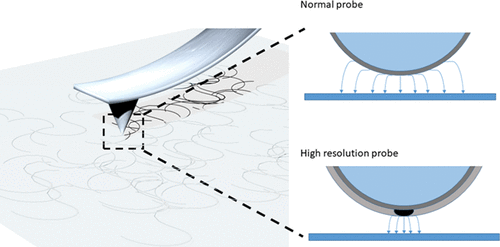
Confining electric fields to a nanoscale region is challenging yet crucial for applications such as high-resolution probing of electrical properties of materials and electric-field manipulation of nanoparticles. State-of-the-art techniques involving atomic force microscopy typically have a lateral resolution limit of tens of nanometers due to limitations in the probe geometry and stray electric fields that extend over space. Engineering the probes is the most direct approach to improving this resolution limit. However, current methods to fabricate high-resolution probes, which can effectively confine the electric fields laterally, involve expensive and sophisticated probe manipulation, which has limited the use of this approach. Here, we demonstrate that nanoscale phase switching of configurable thin films on probes can result in high-resolution electrical probes. These configurable coatings can be both germanium-antimony-tellurium (GST) as well as amorphous-carbon, materials known to undergo electric field-induced nonvolatile, yet reversible switching. By forming a localized conductive filament through phase transition, we demonstrate a spatial resolution of electrical field beyond the geometrical limitations of commercial platinum probes (i.e., an improvement of ∼48%). We then utilize these confined electric fields to manipulate nanoparticles with single nanoparticle precision via dielectrophoresis. Our results advance the field of nanomanufacturing and metrology with direct applications for pick and place assembly at the nanoscale.
中文翻译:

用于纳米工程的丝状高分辨率电探针。
将电场限制在纳米级区域是具有挑战性的,但对于诸如材料电学特性的高分辨率探测和纳米粒子的电场操纵等应用而言,则至关重要。由于探针几何形状的限制和在空间上延伸的杂散电场的限制,涉及原子力显微镜的最新技术通常具有数十纳米的横向分辨率极限。设计探头是提高分辨率极限的最直接方法。但是,目前可以有效地横向限制电场的高分辨率探头的制造方法涉及昂贵且复杂的探头操作,这限制了该方法的使用。这里,我们证明了探针上可配置薄膜的纳米级相转换可以产生高分辨率的电探针。这些可配置的涂层既可以是锗-锑-碲(GST),也可以是非晶碳,这是已知会经受电场感应的非易失性但可逆转换的材料。通过相变形成局部导电丝,我们证明了电场的空间分辨率超出了商业铂探针的几何极限(即提高了约48%)。然后,我们利用这些受限电场通过介电电泳以单个纳米颗粒的精度操纵纳米颗粒。我们的结果直接应用于纳米级的拾放装配,从而推动了纳米制造和计量领域的发展。这些可配置涂层既可以是锗-锑-碲(GST),也可以是非晶碳,这是已知会受到电场感应的非易失性但可逆转换的材料。通过相变形成局部导电丝,我们证明了电场的空间分辨率超出了商业铂探针的几何极限(即提高了约48%)。然后,我们利用这些受限电场通过介电电泳以单个纳米颗粒的精度操纵纳米颗粒。我们的结果直接应用于纳米级的拾放装配,从而推动了纳米制造和计量领域的发展。这些可配置涂层既可以是锗-锑-碲(GST),也可以是非晶碳,这是已知会受到电场感应的非易失性但可逆转换的材料。通过相变形成局部导电丝,我们证明了电场的空间分辨率超出了商业铂探针的几何极限(即提高了约48%)。然后,我们利用这些有限的电场通过介电电泳以单个纳米颗粒的精度操纵纳米颗粒。我们的结果直接应用于纳米级的拾放装配,从而推动了纳米制造和计量领域的发展。通过相变形成局部导电丝,我们证明了电场的空间分辨率超出了商业铂探针的几何极限(即提高了约48%)。然后,我们利用这些受限电场通过介电电泳以单个纳米颗粒的精度操纵纳米颗粒。我们的结果直接应用于纳米级的拾放装配,从而推动了纳米制造和计量领域的发展。通过相变形成局部导电丝,我们证明了电场的空间分辨率超出了商业铂探针的几何极限(即提高了约48%)。然后,我们利用这些受限电场通过介电电泳以单个纳米颗粒的精度操纵纳米颗粒。我们的结果直接应用于纳米级的拾放装配,从而推动了纳米制造和计量领域的发展。
更新日期:2020-01-21
中文翻译:
用于纳米工程的丝状高分辨率电探针。
将电场限制在纳米级区域是具有挑战性的,但对于诸如材料电学特性的高分辨率探测和纳米粒子的电场操纵等应用而言,则至关重要。由于探针几何形状的限制和在空间上延伸的杂散电场的限制,涉及原子力显微镜的最新技术通常具有数十纳米的横向分辨率极限。设计探头是提高分辨率极限的最直接方法。但是,目前可以有效地横向限制电场的高分辨率探头的制造方法涉及昂贵且复杂的探头操作,这限制了该方法的使用。这里,我们证明了探针上可配置薄膜的纳米级相转换可以产生高分辨率的电探针。这些可配置的涂层既可以是锗-锑-碲(GST),也可以是非晶碳,这是已知会经受电场感应的非易失性但可逆转换的材料。通过相变形成局部导电丝,我们证明了电场的空间分辨率超出了商业铂探针的几何极限(即提高了约48%)。然后,我们利用这些受限电场通过介电电泳以单个纳米颗粒的精度操纵纳米颗粒。我们的结果直接应用于纳米级的拾放装配,从而推动了纳米制造和计量领域的发展。这些可配置涂层既可以是锗-锑-碲(GST),也可以是非晶碳,这是已知会受到电场感应的非易失性但可逆转换的材料。通过相变形成局部导电丝,我们证明了电场的空间分辨率超出了商业铂探针的几何极限(即提高了约48%)。然后,我们利用这些受限电场通过介电电泳以单个纳米颗粒的精度操纵纳米颗粒。我们的结果直接应用于纳米级的拾放装配,从而推动了纳米制造和计量领域的发展。这些可配置涂层既可以是锗-锑-碲(GST),也可以是非晶碳,这是已知会受到电场感应的非易失性但可逆转换的材料。通过相变形成局部导电丝,我们证明了电场的空间分辨率超出了商业铂探针的几何极限(即提高了约48%)。然后,我们利用这些有限的电场通过介电电泳以单个纳米颗粒的精度操纵纳米颗粒。我们的结果直接应用于纳米级的拾放装配,从而推动了纳米制造和计量领域的发展。通过相变形成局部导电丝,我们证明了电场的空间分辨率超出了商业铂探针的几何极限(即提高了约48%)。然后,我们利用这些受限电场通过介电电泳以单个纳米颗粒的精度操纵纳米颗粒。我们的结果直接应用于纳米级的拾放装配,从而推动了纳米制造和计量领域的发展。通过相变形成局部导电丝,我们证明了电场的空间分辨率超出了商业铂探针的几何极限(即提高了约48%)。然后,我们利用这些受限电场通过介电电泳以单个纳米颗粒的精度操纵纳米颗粒。我们的结果直接应用于纳米级的拾放装配,从而推动了纳米制造和计量领域的发展。


 京公网安备 11010802027423号