当前位置:
X-MOL 学术
›
ACS Appl. Electron. Mater.
›
论文详情
Our official English website, www.x-mol.net, welcomes your feedback! (Note: you will need to create a separate account there.)
Toward Scalable Fabrication of Atomic Wires in Silicon by Nanopatterning Self-Assembled Molecular Monolayers
ACS Applied Electronic Materials ( IF 4.7 ) Pub Date : 2019-12-31 , DOI: 10.1021/acsaelm.9b00749 Chufan Zhang 1 , Meng Peng 2 , Weida Hu 2 , Yaping Dan 1
ACS Applied Electronic Materials ( IF 4.7 ) Pub Date : 2019-12-31 , DOI: 10.1021/acsaelm.9b00749 Chufan Zhang 1 , Meng Peng 2 , Weida Hu 2 , Yaping Dan 1
Affiliation
|
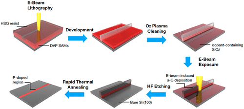
Developing a scalable method to fabricate atomic wires is an important step for building solid-state semiconductor quantum computers. In this work, we developed a selective doping strategy by patterning the self-assembled monolayer to a few nanometers using standard nanofabrication processes, which significantly improves the lateral doping resolution of monolayer doping from microscale to nanoscale. Using this method, we further explore the possibility to fabricate phosphorus wires in silicon by patterning self-assembled diethyl vinylphosphonate monolayers into lines with a width ranging from 500 to 10 nm. The phosphorus dopants are driven into silicon by rapid thermal annealing, forming dopant wires. Four-probe and Hall effect measurements are employed to characterize the dopant wires. The results show that the conductance is linear with the width for the wires, showing the success of the monolayer patterning process to nanoscale. To fabricate atomic wires made of one or a few lines of phosphorus atoms, we need to significantly shorten the thermal diffusion length and increase the dopant incorporation rate at the same time. Pulsed laser annealing may be a promising solution. The present work provides a promising pathway for mass fabrication of atomic wires in silicon that may find important applications in quantum computing.
中文翻译:

通过纳米构图自组装分子单分子膜实现可扩展地制造硅原子线
开发可扩展的方法来制造原子线是构建固态半导体量子计算机的重要步骤。在这项工作中,我们通过使用标准的纳米制造工艺将自组装单层图案化到几纳米,从而开发了一种选择性掺杂策略,这从单级到微米级显着提高了单层掺杂的横向掺杂分辨率。使用这种方法,我们进一步探索了通过将自组装的乙烯基膦酸二乙酯单层图案化为宽度为500至10 nm的线而在硅中制造磷线的可能性。通过快速热退火将磷掺杂剂驱入硅中,从而形成掺杂剂线。采用四探针和霍尔效应测量来表征掺杂剂线。结果表明,电导率与导线的宽度成线性关系,表明单层构图工艺成功地达到了纳米级。为了制造由一或几行磷原子制成的原子线,我们需要同时显着缩短热扩散长度并提高掺杂剂的掺入率。脉冲激光退火可能是有前途的解决方案。本工作为大规模制造硅原子线提供了一种有希望的途径,该途径可能会在量子计算中找到重要的应用。脉冲激光退火可能是有前途的解决方案。目前的工作为硅中原子线的大规模制造提供了一条有希望的途径,这可能会在量子计算中找到重要的应用。脉冲激光退火可能是有前途的解决方案。目前的工作为硅中原子线的大规模制造提供了一条有希望的途径,这可能会在量子计算中找到重要的应用。
更新日期:2020-01-06
中文翻译:
通过纳米构图自组装分子单分子膜实现可扩展地制造硅原子线
开发可扩展的方法来制造原子线是构建固态半导体量子计算机的重要步骤。在这项工作中,我们通过使用标准的纳米制造工艺将自组装单层图案化到几纳米,从而开发了一种选择性掺杂策略,这从单级到微米级显着提高了单层掺杂的横向掺杂分辨率。使用这种方法,我们进一步探索了通过将自组装的乙烯基膦酸二乙酯单层图案化为宽度为500至10 nm的线而在硅中制造磷线的可能性。通过快速热退火将磷掺杂剂驱入硅中,从而形成掺杂剂线。采用四探针和霍尔效应测量来表征掺杂剂线。结果表明,电导率与导线的宽度成线性关系,表明单层构图工艺成功地达到了纳米级。为了制造由一或几行磷原子制成的原子线,我们需要同时显着缩短热扩散长度并提高掺杂剂的掺入率。脉冲激光退火可能是有前途的解决方案。本工作为大规模制造硅原子线提供了一种有希望的途径,该途径可能会在量子计算中找到重要的应用。脉冲激光退火可能是有前途的解决方案。目前的工作为硅中原子线的大规模制造提供了一条有希望的途径,这可能会在量子计算中找到重要的应用。脉冲激光退火可能是有前途的解决方案。目前的工作为硅中原子线的大规模制造提供了一条有希望的途径,这可能会在量子计算中找到重要的应用。


 京公网安备 11010802027423号