当前位置:
X-MOL 学术
›
ACS Appl. Nano Mater.
›
论文详情
Our official English website, www.x-mol.net, welcomes your feedback! (Note: you will need to create a separate account there.)
Hot Electron Generation in Silicon Micropyramids Covered with Nanometer-Thick Gold Films for Near-Infrared Photodetectors
ACS Applied Nano Materials ( IF 5.9 ) Pub Date : 2020-01-13 , DOI: 10.1021/acsanm.9b01840 Yusheng Zhai 1 , Yupei Li 1 , Jitao Ji 1 , Zhipeng Wu 1 , Qilong Wang 1
ACS Applied Nano Materials ( IF 5.9 ) Pub Date : 2020-01-13 , DOI: 10.1021/acsanm.9b01840 Yusheng Zhai 1 , Yupei Li 1 , Jitao Ji 1 , Zhipeng Wu 1 , Qilong Wang 1
Affiliation
|
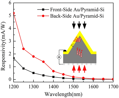
Plasmonic metallic nanostructure/silicon composites are gaining increasing attention due to their NIR photodetection capability and potential compatibility with CMOS technology. However, those kinds of photodetectors suffer from low efficiency due to the low optical absorption and poor hot electron injection efficiency. Here, we propose an efficient and low-cost NIR photodetector based on a gold film coated silicon micropyramid, which was fabricated with the large-scale, lithography-free, chemical wet-etching process. We experimentally demonstrated that the proposed micropyramid enhanced the photoresponsivity for the NIR light by 3 times compared with that of the flat reference sample at 1300 nm. Besides, the micropyramid strategy allowed the photodetector to preserve the polarization-insensitive and incident-angle-insensitive photoresponse. Furthermore, we further increased the responsivity through the back-side illumination from the silicon side and carefully investigated the background mechanism by changing the thickness of the covered gold film. It is demonstrated that the enhanced responsivity is related to the location of the field enhancement (hot spots); the nearer to the Au/silicon interface, the higher the responsivity. These results indicate that the location of hot spots has a significant contribution to the hot electron injection efficiency and responsivity, and the simple wet-etching method is promising for large-scale and low-cost plasmonic hot-electron-based NIR photodetectors.
中文翻译:

覆盖纳米级金膜的近红外光电探测器用硅微金字塔中的热电子生成
等离子体金属纳米结构/硅复合材料因其近红外光检测能力和与CMOS技术的潜在兼容性而受到越来越多的关注。然而,由于低的光吸收和较差的热电子注入效率,这些类型的光电探测器效率低。在这里,我们提出了一种高效且低成本的基于金膜涂覆的硅微金字塔的近红外光电探测器,该探测器是通过大规模,无需光刻的化学湿蚀刻工艺制成的。我们通过实验证明,所提出的微金字塔对近红外光的光响应性比平坦参比样品在1300 nm处提高了3倍。此外,微金字塔策略使光电探测器可以保留对偏振不敏感和对入射角不敏感的光响应。此外,我们通过从硅侧进行的背面照明进一步提高了响应度,并通过更改被覆金膜的厚度仔细研究了背景机制。结果表明,增强的响应度与场增强(热点)的位置有关;距Au /硅界面越近,响应度越高。这些结果表明,热点的位置对热电子注入效率和响应度有重大贡献,并且简单的湿法刻蚀方法有望用于大规模和低成本的基于等离激元热电子的NIR光电探测器。我们通过从硅侧进行的背面照明进一步提高了响应度,并通过更改被覆金膜的厚度仔细研究了背景机制。结果表明,增强的响应度与场增强(热点)的位置有关;距Au /硅界面越近,响应度越高。这些结果表明,热点的位置对热电子注入效率和响应度有重大贡献,并且简单的湿法刻蚀方法有望用于大规模和低成本的基于等离激元热电子的NIR光电探测器。我们通过从硅侧进行的背面照明进一步提高了响应度,并通过更改被覆金膜的厚度仔细研究了背景机制。结果表明,增强的响应度与场增强(热点)的位置有关;距Au /硅界面越近,响应度越高。这些结果表明,热点的位置对热电子注入效率和响应度有重大贡献,并且简单的湿法刻蚀方法有望用于大规模和低成本的基于等离激元热电子的NIR光电探测器。
更新日期:2020-01-13
中文翻译:
覆盖纳米级金膜的近红外光电探测器用硅微金字塔中的热电子生成
等离子体金属纳米结构/硅复合材料因其近红外光检测能力和与CMOS技术的潜在兼容性而受到越来越多的关注。然而,由于低的光吸收和较差的热电子注入效率,这些类型的光电探测器效率低。在这里,我们提出了一种高效且低成本的基于金膜涂覆的硅微金字塔的近红外光电探测器,该探测器是通过大规模,无需光刻的化学湿蚀刻工艺制成的。我们通过实验证明,所提出的微金字塔对近红外光的光响应性比平坦参比样品在1300 nm处提高了3倍。此外,微金字塔策略使光电探测器可以保留对偏振不敏感和对入射角不敏感的光响应。此外,我们通过从硅侧进行的背面照明进一步提高了响应度,并通过更改被覆金膜的厚度仔细研究了背景机制。结果表明,增强的响应度与场增强(热点)的位置有关;距Au /硅界面越近,响应度越高。这些结果表明,热点的位置对热电子注入效率和响应度有重大贡献,并且简单的湿法刻蚀方法有望用于大规模和低成本的基于等离激元热电子的NIR光电探测器。我们通过从硅侧进行的背面照明进一步提高了响应度,并通过更改被覆金膜的厚度仔细研究了背景机制。结果表明,增强的响应度与场增强(热点)的位置有关;距Au /硅界面越近,响应度越高。这些结果表明,热点的位置对热电子注入效率和响应度有重大贡献,并且简单的湿法刻蚀方法有望用于大规模和低成本的基于等离激元热电子的NIR光电探测器。我们通过从硅侧进行的背面照明进一步提高了响应度,并通过更改被覆金膜的厚度仔细研究了背景机制。结果表明,增强的响应度与场增强(热点)的位置有关;距Au /硅界面越近,响应度越高。这些结果表明,热点的位置对热电子注入效率和响应度有重大贡献,并且简单的湿法刻蚀方法有望用于大规模和低成本的基于等离激元热电子的NIR光电探测器。


 京公网安备 11010802027423号