Abstract
We present results exploring different concepts for Pb monolayer mediated thin film growth of Cu on Ru(0001) and Co on polycrystalline Cu substrates. Both systems are of considerable importance in microchip fabrication technology and they exhibit a three dimensional growth at room temperature which somewhat limits their application. The Pb monolayer mediation of the growth process is explored by having its role as a surfactant, flux mediator or as a sacrificial layer in deposition via surface limited redox replacement protocol. Electrochemical and STM results suggest that Pb monolayer induces 2D Cu growth on Ru(0001) and the growth mechanism is very dependent on the Pb mediation role. The surfactant properties of electrolessly deposited Pb monolayer are also studied during electroless deposition of Co on polycrystalline Cu. The benefit of Pb monolayer mediation of the Co growth process was manifested by 2D Co thin film morphology, high quality of the grain boundaries, and improved magnetic properties.
Export citation and abstract BibTeX RIS

This is an open access article distributed under the terms of the Creative Commons Attribution 4.0 License (CC BY, http://creativecommons.org/licenses/by/4.0/), which permits unrestricted reuse of the work in any medium, provided the original work is properly cited.
Properties of heteroepitaxial thin films are often dependent on the method and conditions used for deposition.1 In that respect, the electrochemical growth represents energetically different approach as compared to conventional vacuum deposition methods. In some instances it offers a unique advantages which can be exploited in order to get high quality thin films. The obvious one is that electrochemical growth is the ambient temperature process representing the opportunity to grow many heteroepitaxial metal overlayers while preserving the integrity of their interface. However, in many substrate-overlayer systems, the thermodynamics as well as growth kinetics at ambient conditions favor nucleation and growth of rough 3D films with limited applications.2–4 In recent years, a significant progress has been made in understanding the kinetic aspects controlling the thin film growth modes.5–7 Various approaches to manipulate growth kinetics and enhance the evolution of atomically flat epitaxial overlayers were discovered.8–10 Some of these findings have been successfully implemented for electrochemical thin film growth resulting in several new deposition protocols such as Defect Mediated Growth (DMG),11,12 Surfactant Mediated Growth (SMG)13 and growth via Surface Limited Redox Replacement (SLRR).14,15 The common phenomenon among these protocols is that two-dimensional (2D) thin film growth is induced by mediation of the growth process using underpotentially deposited (UPD) monolayer (ML).
In this paper we report results exploring different concepts for Pb ML mediated thin film growth of Cu on Ru(0001) and Co on polycrystalline Cu (Cu(hkl)) substrates. Both heteroepitaxial systems are of great significance for microchip fabrication technology where 2D growth is preferred.16–18 However, at room temperature, both systems exhibits a 3D growth.19–21 The growth of Cu on Ru(0001) proceeds with Cu UPD ML formation which is followed by immediate transition to 3D growth in overpotential region (OPD),19,20,22,23 Figure 1. In our work, the Pb ML mediation is explored having the role of Pb ML serving either as a surfactant (SMG), flux mediator (DMG) or as a sacrificial layer in deposition via SLRR protocol. In each case, a 2D growth of Cu films on Ru(0001) is induced. The beneficial role of Pb ML as mediator is also studied during the electroless (e-less) deposition of Co thin film on Cu(hkl). The Pb ML is e-lessly deposited on Cu(hkl) substrate which served as surfactant during the e-less Co deposition. The benefit of Pb ML mediation of the Co growth process was manifested by 2D Co thin film morphology, higher density of the grain boundaries, and improved magnetic properties.
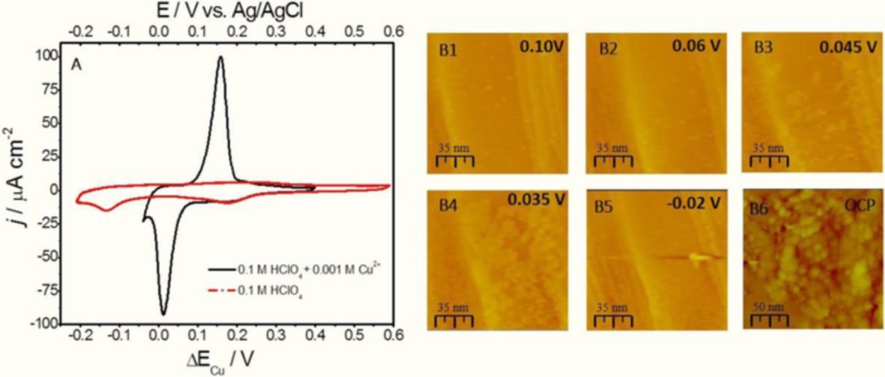
Figure 1. (A) Cyclic Voltammogram for Ru(0001) in 0.1 M HClO4 + 0.001 Cu2+ (black) and 0.1 M HClO4 (red). Potential indicated with respect to ΔECu. (bottom axis) and Ag/AgCl (top axis), dE/dt = 0.02 Vs−1. (B1-B5) In situ STM of Cu UPD on Ru (0001). Potential during STM image acquisition and scale bar are indicated in each image. (B6) Morphology of the Cu deposit on Ru(0001) obtained at −0.2 V after 5 minutes of growth. Potential in images indicated with respect to ΔECu.
Experimental
General details
The starting Ru(0001) was disk with diameter 10 mm and 2 mm thickness, (Monocrystals Company). It was prepared using mechanical polishing and induction annealing in 75%H2+24%N2+1%CO gas mixture at 1400°C for 60 min. This routinely yielded a highly reflective mirror-like surface with very reproducible Cu UPD voltammetry (Figure 1A). The Cu polycrystalline substrates were 100 - 200 nm thick films deposited on SiO2/Si wafer and reduced in the same gas mixture at 250°C for 15 minutes unless otherwise stated in the text. All solutions for Cu and Pb UPD ML deposition, Cu and Co deposition and SLRR reaction were prepared with high purity grade chemicals (99.999%, Alfa Aaeser, Merck) and >18.2 MΩ ultra-pure water (Millipore Direct Q-UV with Barnstead A1007 pre-distillation unit). Before each experiment, solutions were de-aerated for one hour with ultrapure nitrogen in order to minimize concentration of dissolved oxygen from air. All experiments are performed using ultraclean glassware and in oxygen-free environment. The volume of the electrochemical cell was 0.150 dm3 while the amount/volume of the reaction solution was standardized to 0.1 dm3 for each experiment. The volume of the solution during insitu scanning tunneling microscopy (STM) studies was 0.001 dm3. In the case of Ru(0001) crystal, the hanging meniscus electrode configuration was used for electrochemical studies. In the case of Cu films, the samples were simply immersed into the solution. All potentials in the text are presented either as the value of Cu-underpotential, ΔECu or as a potential vs. silver-silver chloride reference electrode (Ag/AgCl/1.0 M KCl; E = 0.235 V vs. SHE). The electrochemical studies were performed using BASi Epsilon system, while insitu and exsitu STM and AFM images were recorded using Nanoscope V controller with multimode scanner unit (Veeco instruments). The STM tips were made of PtIr wire coated with apiezon wax to minimize faradaic current contribution to the tunneling signal. The solution for e-less Pb ML deposition was prepared by mixing two volume parts of the solution containing Pb2+ ions (Pb(ClO4)2) and one volume part of the solution containing V2+ ions as reducing agent (VCl2). Both solutions contained 0.1 M HClO4 as a background electrolyte. The nominal concentrations of Pb2+ and V2+ in solution for e-less Pb ML deposition are presented in Table I. The solution for e-less Co deposition has been discussed in the patent literature24 and, in our work, we used similar formulation which is propriety of Lam Research Corporation. The main reducing agent for Co e-less deposition was Ti3+ ion (TiCl3) yielding Co deposition rate of 0.01–0.012 nms−1 on different substrates (Cu, Ru, Au). In our work, we limit discussion on Co e-less deposition on Cu and the description of solution for e-less Cu deposition25 is shown in Table I.
Table I. Solutions for the e-less Pb ML deposition, and e-less Cu deposition.25
| e-less Pb monolayer Dep. | e-less Cu Deposition |
|---|---|
| 0.1 M HClO4 | 0.05 M CuCl2 |
| 0.001/0.00066 M Pb2+ | 0.15 CoCl2 |
| 0.003 M V2+ | Ethylenediamine 1.2 M |
| 0.0003 M Cl− | pH ≈ 6 (adjusted with HCl) |
| Nom. rate: 2 nms−1 |
Experimental routine for e-less Pb ML deposition and mediated e-less Co growth
All deposition experiment and the open circuit potential (OCP) measurements during the e-less Pb ML deposition were performed in N2 filled glove box using Cu polycrystalline films as substrates. The entire experiment involved three steps. They are briefly explained below:
- (1)Step one: First, the cyclic voltammetry measurements were performed to verify the quality of the surface and characteristics of the Pb UPD process on a Cu(hkl) surface.
- (2)Step two: The potential is switched to the open circuit and OCP transients are recorded during the addition of V2+ containing aliquot. Typical length of the OCP measurements was between 50–100 seconds.
- (3)Step three: The sample with deposited e-less Pb ML is transferred to a well de-aerated 0.1 M HClO4 solution and the linear sweep is performed in anodic direction to strip the Pb ML and record the stripping charge.
The same experimental routine is also performed during the e-less Co growth with Pb ML serving as surfactant, except that the third step was omitted and the sample was transferred/immersed to the solution for e-less Co deposition.
In the case of the multilayer growth of Co/Cu giant magnetoresistance stack (GMR), the custom made automated set up for e-less atomic layer deposition (ALD) was used. The sample resided on the spinning platform which was synchronized with 3 solutions dispensers on top of the sample and all of them were integrated into a computer controlled loop. During exposure of the sample to the e-less Pb ML deposition solution, rinsing solution (H2O), e-less Cu and Co deposition solutions, sample was kept stagnant for certain time to allow the specific thickness of Co, Cu or Pb ML deposition to occur. However, in between each solution exposure step in the single ALD cycle, the sample was spun at 400 rpm to remove either solution. This way, a completely automated deposition of an arbitrary number of e-less ALD cycles was performed without any human intervention.
Results and Discussion
Cu/Ru(0001) system
Recently, new barrier layer materials have been considered to replace the commonly used Ta, Ti- based barriers for seedless copper deposition in the damascene process.26–28 Among different candidates Ru has attracted the most interest as a new barrier material or barrier liner (Ru/TaN, Ru/TiSiN...) owing to its favorable intrinsic properties. A number of electrochemical19,20,22 studies of initial stages of Cu deposition on Ru have shown complete wetting with epitaxial and strained monolayer(s) at the initial stage followed by Stranski-Krastanov growth mode at higher thickness.
In Figure 1A, the characteristic cyclic voltammogram (CV) of Cu UPD on freshly prepared Ru(0001) is shown (black). One can distinguish large cathodic peak centered at 0.02 V ΔECu, which is preceded by the smaller shoulder peak centered at ≈0.2 V. The CV of freshly prepared Ru(0001) surface in 0.1 M HClO4 solution is also shown by red line in Figure 1A and indicates that the shoulder peak of the Cu UPD process is related to the Ru-surface oxide/hydroxide reduction.29 The second reduction peak of the Ru-surface oxide/hydroxide occurs at more negative potential which falls into the overpotential deposition (OPD) region of Cu. Therefore, we can conclude that the entire Cu UPD process is confined within the electrochemical signal of the main cathodic peak at 0.02 V ΔECu,. It is also apparent that the Cu UPD ends at the potential of −0.02 V which slightly enters into the OPD range of Cu. During anodic sweep, the Cu UPD ML stripping peak is observed at 0.165 V ΔECu, This is about 0.145 V more positive than the potential of the Cu UPD peak and suggests an irreversibility of the UPD process. The possible reason for this is simultaneous Ru-surface reduction/oxidation and Cu underpotential deposition/stripping which cause the energetics of the adsorption sites on Ru surface to change significantly between the cathodic and anodic sweep.
In order to gain more insight of the Cu/Ru(0001) system growth mode we have performed the in situ STM experiment during Cu UPD and OPD growth. The results are shown in Figure 1B, The image B1 shows the morphology of the Ru(0001) at the 0.1 V ΔECu, just prior to the Cu UPD peak. The ≈70 nm wide terraces and monoatomic steps are evident with some small clusters which are likely the residue of the Ru-hydroxide/oxide reduction from terrace sites discussed previously (peak at 0.2 V ΔECu). Entering into the bottom of the Cu UPD peak at 0.06 V (image B2), some contrast changes at the steps are observed as well as increasing population of small clusters on the terraces. The height of these clusters is below Cu atomic diameter, and those are attributed to the residue of the further Ru-oxide/hydroxide reduction at the terraces sites. As the potential is stepped to the mid-range of the UPD peak (images B3 and B4) the Cu nucleation and growth is evident on the terraces and gradual filling of the Cu UPD ML. One interesting observation is that no preferential growth of Cu UPD ML is observed at the steps, but rather its exclusive nucleation on the terraces. This indicates that the steps maybe still passivated by the presence of strongly bonded hydroxyl spices. Stepping the potential into the OPD region at −0.02 V, where the UPD peaks ends (Figure 1A), the Cu UPD ML densifies and completes on the terraces. However, as the STM scan progresses, the onset of the Cu 3D growth is observed originating at the step (image B5). Results in Figure 1B reconfirm the previous literature reports for Cu/Ru system exhibiting SK growth.20 An interesting findings in our study are that we do see that the transition from 2D UPD ML growth to 3D OPD growth starts at the step edges, rather than as nucleation of the 3D islands at the terraces. The possible reason is that the Ru-surface is not completely free from the Ru-hydroxide/oxide in the potential range of the Cu UPD/OPD transition. The second reduction peak on Ru surface occurs at the potential of −0.15 V ΔECu which suggest that reduction of the Ru surface at this potential is likely related to reduction of the most stable Ru-oxide/hydroxide at the defects and step sites on the Ru surface. Therefore, presence of the oxide/hydroxide at steps can be additional barrier for Cu adatoms step-down process resulting in the 2D-3D growth mode transition. Because of that, the Cu OPD experiment in STM cell is conducted at the −0.2 V ΔECu, which is the potential where Ru surface should be free from any oxide. Then, the potential control is turned off, and the STM image is recorded showing 3D Cu morphology (image B6). Obviously, the presence of residual oxide at the steps cannot be attributed as the only cause for Cu 3D growth on Ru(0001). The growth kinetics and strain play an important role too as we have routinely observed 3D growth of Cu at any OPD potential more negative than second peak for Ru-oxide/hydroxide reduction, (−0.15 V ΔECu,).
Surfactant mediated growth (SMG)
The protocol employed in SMG is inspired by earlier vacuum deposition work of Camarero et al.9 demonstrating layer-by-layer growth of Cu on Pb ML covered Cu(111) at 300 K. The applicability of SMG in electrochemical system is first demonstrated by 2D growth of more than 200 MLs Ag on Au (111) and for the epitaxial growth of more than 50 MLs of Cu on Cu (111).13,30 During SMG experiments, the Pb layer (surfactant) coverage was controlled strictly by the applied potential in the Pb UPD region for Cu substrate. The study is conducted using two different solution formulations. In the first case, Figure 2, the Cu concentration was relatively high, 10−3 M, where the Cu growth occurs under mixed control providing a large Cu deposition flux (≈0.06 MLs−1). In Figure 2A, the CV for Ru(0001) surface is shown in solution corresponding to the conditions during the SMG growth experiment (0.1 M HClO4 + 0.1 M Pb2+ + 10−3 M Cu2+). In the cathodic sweep of the CV one can see the features of the Cu UPD process on Ru(0001) discussed earlier which include shoulder peak at ≈+0.18 V and the main Cu UPD peak at ≈0.02 V vs. Ag/AgCl. However, proceeding further in the Cu OPD range, the additional cathodic peak at – 0.1 V, corresponds to Pb UPD on the growing Cu layer on Ru(0001). Upon reversal of the scan direction, the anodic sweep reveals Pb UPD stripping peak at 0.05 V which has about the same charge as the Pb UPD peak and the Cu stripping peak at 0.2 V. The Cu stripping peak has significantly larger charge than the Cu UPD peak. Obviously, the signal form the bulk Cu stripping and Cu UPD ML striping are convoluted under the one Cu stripping peak at this scan rate (dE/dt = 0.05 Vs−1) although the vague shoulder on the negative side of the Cu stripping peak does indicate two thermodynamically different processes.
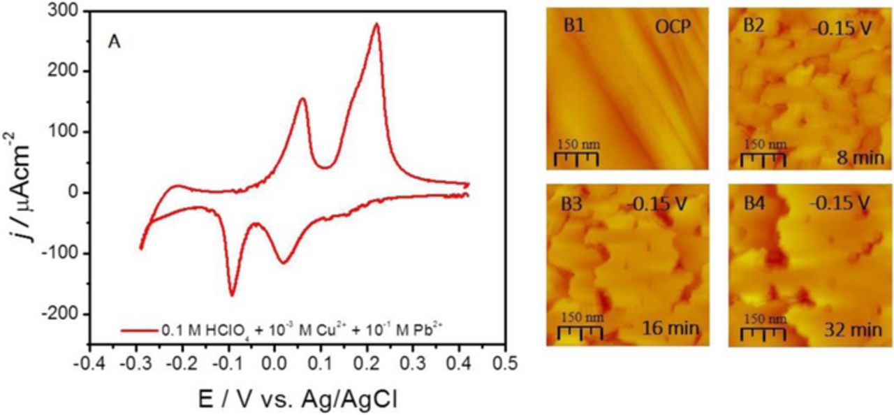
Figure 2. (A) Cyclic Voltammogram for Ru(0001) in 0.1 M HClO4 + 0.001 Cu2+ 0.1 M Pb2+, dE/dt = 0.05 Vs−1. (B1-B4) In situ STM of SMG of Cu on Ru (0001) using Pb UPD ML as a surfactant. Potential during STM image acquisition and scale bar are indicated in each image. Potential indicated with respect to Ag/AgCl.
According to the CV, Figure 2A, the potential for the Cu OPD growth during in situ STM experiment was chosen to be in the range where the full Pb UPD ML is present on the growing Cu surface (ESMG = −0.15 V vs. Ag/AgCl). The in situ STM images of the Cu SMG are shown in Figure 2B. The starting Ru(0001) surface, image B1, is at OCP and the time-resolved evolution of the growing Cu surface morphology is shown in images B2-B4 at – 0.15 V. It is obvious that the 2D Cu growth occurs at a very fast rate, therefore STM shows quite large changes of the surface morphology during acquisitions of subsequent images. The image acquisition time (≈200 sec/image) is too slow to observe the details of the nucleation and growth process, yet it is evident that the most of the morphology change is dominated by the fast moving steps. The estimated amount of Cu deposited during acquisition of one image is ≈10 ML. However, one can anticipate a lower deposition rate in the region confined between the sample surface and the STM tip. Regardless, the surface morphology shown in one STM image represent a composed time evolution of the Cu surface morphology change between the first and the last scan line. Having this in mind, the 2D outlook of the growing Cu surface appears even more fascinating and illustrates the best way a fundamental change of the Cu growth mode induced by the presence of the Pb UPD ML. A simple comparison between the image B6 in Figure 1B and image B4 in Figure 2B yields the same conclusion.
In order to observe more details of the Cu SMG, in the second in situ STM experiment, Figure 3, the Cu concentration was much smaller, 5 × 10⁻⁵ M, and the Cu growth occurred under transport limited conditions with significantly lower deposition flux (0.005 MLs−1). The CV of the Ru(0001) for corresponding SMG solution is shown in Figure 3A (0.1 HClO4 + 5 × 10⁻⁵ M Cu2+ + 0.01 M Pb2+). The low concentration of Cu2+ and transport limited deposition regime leads to not well defined Cu UPD peak at 0.035 V in cathodic scan as compared to Figure 1A and Figure 2A. The formation of full Cu UPD ML at this scan rate (dE/dt = 0.05 Vs−1) is delayed until the applied potential enters the range of the Cu OPD (E < −0.03 V). Because of that, the Cu UPD ML completion and Pb UPD ML formation on top occur simultaneously and the current signals from these two processes are convoluted under the peak at −0.07 V (Pb UPD peak). In addition to that, the Pb UPD peak at −0.07 V appears quite larger than the Pb UPD ML stripping peak at 0.05 V while the charge of the second stripping peak, i.e. Cu stripping peak at 0.16 V, corresponds mainly to the Cu UPD ML stripping with very modest contribution from the Cu deposited in the OPD region (≈0.04 ML).
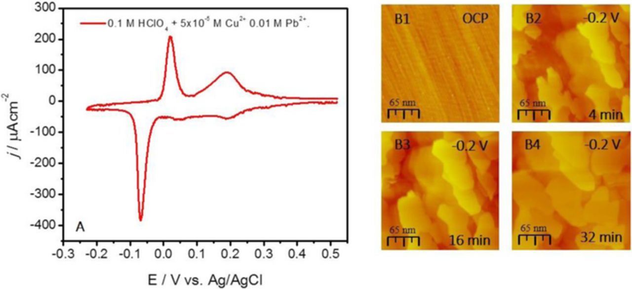
Figure 3. (A) Cyclic Voltammogram for Ru(0001) in 0.1 M HClO4 + 5 × 10⁻⁵ M Cu2+ 0.01 M Pb2+, dE/dt = 0.05 Vs−1. (B1-B4). In situ STM images during SMG of Cu on Ru (0001) using Pb UPD ML as a surfactant. Potential during STM image acquisition and scale bar are indicated in each image. Potential indicated with respect to Ag/AgCl.
The sequence of in situ STM images during the Cu SMG in the solution corresponding to the CV in Figure 3A is shown in Figure 3B. The Cu growth is conducted at −0.2 V which is more negative potential than in the previous experiment. This potential is chosen in order to compensate the negative shift in the Cu reversible potential due to lower Cu ion concentration and to have a comparable overpotential conditions for Cu nucleation and growth in both experiments. In image B1, the starting Ru(0001) surface is displayed. A large density of steps is evident with very small terraces (3–5 nm in width). Upon application of the SMG potential, the image B2 shows progression of the 2D Cu growth characterized by evolution of the multiple 2D plates/clusters originating from the Ru steps. Further growth proceeds by simultaneous 2D growth of Cu plates at different levels. They are characterized by 50–100 nm wide terraces and monoatomic steps (B3-B4). No nucleation of Cu on top of the growing 2D clusters is observed within the time frame of the image acquisition but rather a fast lateral growth via step flow. In image B4, one can see a gradual merger of the large Cu clusters/plates into a semi-complete layers. The nominal thickness of the Cu layer in image B4 is ≈10 ML or 3 nm. A very slow deposition rate renders the Cu surface to be close to equilibrium which is indicated by presence of 2D clusters with edge angles of 60° and 120°. Importantly, these angles correspond to the low index directions of the (111) surface which confirms that the SMG produces the epitaxial Cu layer on Ru(0001). Image B4 in Figure 3B is qualitatively similar to image B4 in Figure 2B and they both show fundamentally different morphology from image B6 in Figure 1B. Therefore, the SMG produces a Cu films with 2D morphology for a wide range of Cu ion concentration. The XPS analysis of the Cu thin films indicates that a small amount of Pb remains in the Cu deposit. In the case of the experiment with larger deposition flux, the amount of Pb is found to be 7 at % (Figure 2). In the case of the experiment with a lower deposition flux, the Pb amount is much lower, ≈2 at % (Figure 3). In conclusion, we can state that the full Pb UPD ML serving as a surfactant during Cu SMG changes the growth mode of Cu from 3D to 2D and the growth occurs mainly by nucleation at the Ru step edges and proceeds further by lateral growth of the Cu clusters via facile step flow. Yet, the optimum Pb UPD ML coverage producing the purest Cu deposit and 2D growth is probably different than what is shown in this study.
Defect mediated growth (DMG)
The strategy used to manipulate the growth kinetics in DMG is based on UHV deposition experiments examining Ag/Ag(111) homo-epitaxy.4 In this approach, the metal of interest is co-deposited with a reversibly deposited mediator metal. The mediator is periodically deposited and stripped from the surface by appropriate cycling of the electrochemical potential while the metal of interest is steadily depositing. Each cycle creates new population of nuclei on the surface and makes the ones developed in previous cycles grow bigger until they merge in continuous layer.11,12
In Figure 4A, the CV for Ru(0001) in solution used for DMG experiment is shown (0.1 M HClO4 +10−4 M Cu2+ 0.01 M Pb2+). As in the previous cases (Figure 2A and Figure 3A), during the cathodic scan, the characteristic peaks corresponding to Cu UPD on Ru(0001) at 0.0 V and Pb UPD on growing Cu surface at −0.12 V vs. Ag/AgCl are observed. The Cu2+ concentration is low, 10−4 M which provides a transport limited conditions for Cu OPD growth. Thus, the Cu deposition rate in the OPD region is potential independent (const) and measured to be ≈0.02 MLs−1. The Pb UPD ML stripping peak and Cu stripping peaks are observed in the anodic scan at −0.04 V and 0.1 V respectively. The limits of the potential sweep during the DMG protocols were chosen to be between the potential range of the full Pb UPD ML formation (−0.2 V) and the onset of the Cu stripping peak (0.0 V). The sweep rate during the Cu DMG was 0.2 Vs−1. The design of the optimum sweep rate for DMG involved ex situ measurements of the Cu thin film surface reflectivity after 10 nm of Cu on Ru(0001) was grown using sweeps ranging from 1Vs−1 to 0.1 Vs−1. The sweep of 0.2 Vs−1 was found to produce Cu deposit with the highest surface reflectivity. At this sweep rate, the Pb UPD ML deposition/dissolution occurred with frequency of 0.5 Hz and the in situ methodology for Cu growth monitoring using STM as presented in Figures 1–3 was an experimental challenge. For this reason, the results for Cu DMG were evaluated using the ex situ STM images recorded upon the DMG experiment was completed. In Figure 4B, image B1, represents the surface morphology of ≈3 nm Cu film on Ru(0001) obtained by DMG protocol described previously. The 2D morphology of Cu is characterized with large population of small clusters on flat terraces (5–10 nm wide) separated by monoatomic steps. The overall outlook of the surface is 2D, and the STM image reveals that 2D clusters are only partially merged into a semi-complete layers. The images B2 and B3 are recorded insitu during the Cu film dissolution whose surface is presented in image B1 (E = OCP). The gradual dissolution of Cu layer reveals the morphology of the underlying Ru(0001) surface, image B3. In order to keep the focus on the same position on the Ru surface, the STM tip was retained at imaging mode and with the same scan size but the scan rate was slowed down to 0.1 Hz. Then, the new Cu DMG experiment is performed for 5 minutes to grow again the Cu thin film with approximate thickness of 3 nm.
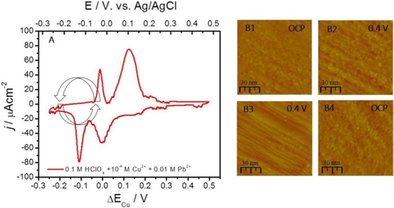
Figure 4. (A) Cyclic Voltammogram for Ru(0001) in 0.1 M HClO4 + 10−4 M Cu2+ + 0.01 M Pb2+, dE/dt = 0.02 Vs−1. (B1 and B4) The STM image of ≈3 nm Cu layer on Ru (0001) grown using Pb UPD ML as a mediator and DMG protocol. Potential sweep limits during DMG were between −0.2 V and 0.05 V ΔECu and they are indicated in the CV. (B2 and B3). The in situ STM images during dissolution of Cu layer on Ru (0001) grown using DMG protocol and Pb UPD ML as a mediator. Potential during STM image acquisition and scale bar are indicated in each image.
Upon the growth termination, the STM image is recorded (image B4) showing the morphology of the Cu thin film at the same spatial position as the image B3. The 2D outlook of Cu film surface is obvious, and more importantly, there is a great deal of morphological similarity between the Cu surface in image B1 and in image B4 which is another indication of the 2D growth. In addition, it has to be mentioned that the morphology of the underlying Ru(0001) surface shown in image B3 does transpires in the morphology of the Cu surface in both images; B1 and B4. This is a clear indicator of the true 2D Cu growth induced by the DMG protocol. However, the Cu thin film morphology obtained by DMG is quite different than the Cu surface morphology obtained by SMG protocol (Figure 2 and Figure 3). Obviously, the Pb UPD ML mediation process during DMG protocol induces an enhanced 2D nucleation of Cu resulting in the 2D thin film morphology different than the one produced by SMG protocol. Importantly, the 2D clusters which partially merge in to a layers at different levels, do replicate the underlying Ru surface which was not the case with Cu films obtained by SMG protocol.
Cu growth via SLRR of Pb UPD ML
Deposition via SLRR of UPD ML14 has gained a lot of attention and applications in last two decades.15,31,32 The main idea is to use an UPD ML as sacrificial material to reduce/deposit a more noble metal (SLRR reaction i.e. galvanic displacement). The most recently developed SLRR protocol so called "one-solution, one-cell" design33,34 is particularly well suited for thin film growth application. In this protocol, the same solution serves for UPD ML formation and subsequent SLRR reaction at open circuit potential. The same protocol is used in this study and the schematics of the experimental steps is shown in Figure 5A. The single SLRR cycle assumes a sequence of potential controlled step, where co-deposition of Pb UPD ML with small amount of Cu occurs, and the open circuit step, where the SLRR reaction and deposition of Cu proceeds. It has to be mentioned that in the first cycle, the Pb UPD occurs on Ru surface partially covered by Cu UPD ML, while in subsequent cycles, as the Cu film covers the Ru surface, the Pb UPD occurs on Cu/Ru(0001) surface.35 The main parameters of the growth protocol are Pb UPD ML formation potential, EPb-UPD, and duration of this step, Δt1, and the duration the OCP step, Δt2, where actual SLRR reaction between Cu2+ and Pb UPD ML occurs, Figure 5A. The solution design used in this experiment and corresponding CV are the same as the one discussed previously for DMG growth in Figure 4A.
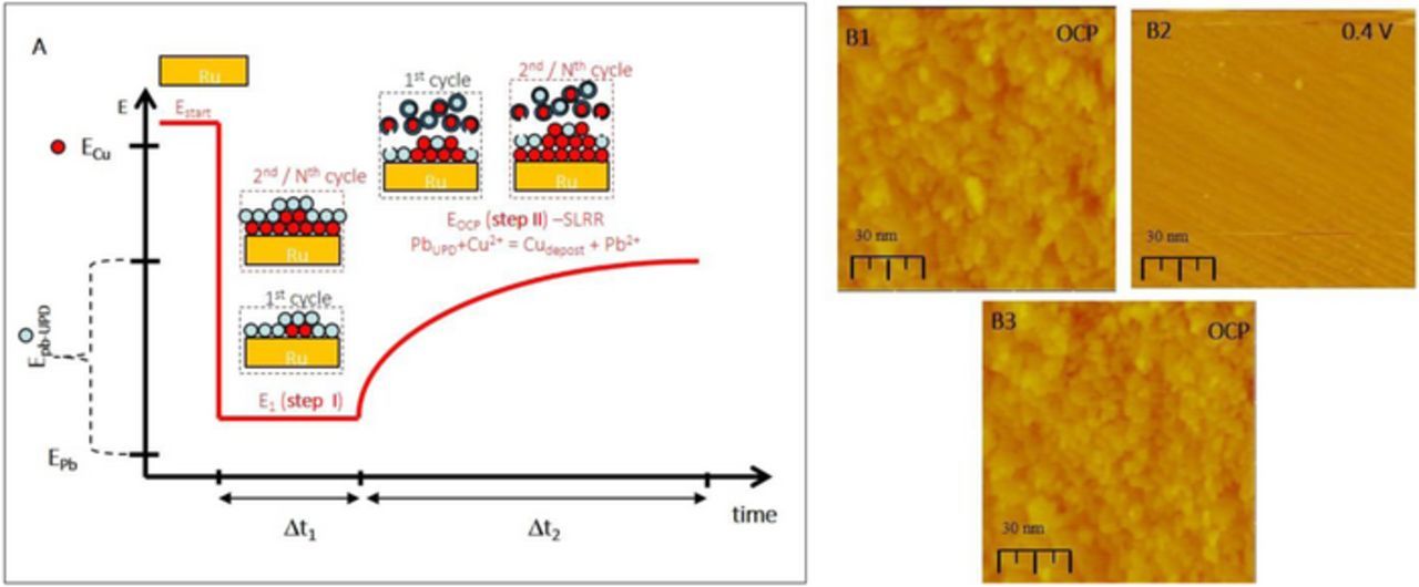
Figure 5. (A) Schematics of the Cu growth on Ru(0001) via SLRR of Pb UPD ML (one cycle). Red-Cu atoms, blue-Pb atoms. (B1 and B3) Morphology of ≈10 nm Cu on Ru(0001) grown via SLRR of Pb UPD ML after 30 cycles from solution: 0.1 M HClO4 +10−4 M Cu2+ 0.01 M Pb2+. Parameters of the Cu growth are: Δt1 = 3 s, Δt2 = 60 s, E1 = −0.2 V, 30 cycles. (B2) Morphology of underlying Ru(0001) after the Cu layer shown in B1 is dissolved at 0.4 V. Potential during STM image acquisition and scale bar are indicated in each image. Potentials are quoted with respect to Ag/AgCl.
In Figure 5B, the STM image B1 shows the morphology of the Cu layer on Ru(0001) deposited in 30 repetitive SLRR cycles using parameters of the SLRR protocol described in figure captions. One can see that the Cu surface displays 2D morphology characterized by short terraces, 10–20 nm wide, which are stacked in many consecutive layers and separated by monoatomic steps. In some instances, the 2D islands are visible on the Cu terraces which are probably residue from not fully grown and merged 2D Cu nuclei i.e. incomplete layers. The outlook of this 2D Cu surface morphology is quite different than the one shown in Figure 4 (DMG) and in Figure 3 (SMG) although the simple comparison is not easy since here we have different thickness of the Cu film (10 nm). However, one thing that transpires is that the surface morphology of the Cu film grown via SLRR of Pb UPD ML in terms of the density of 2D nuclei on the surface appears to be between the morphologies observed in the case of SMG, Figure 3B (no nuclei) and in the case of DMG, Figure 4B (many 2D nuclei). Thus, one can assume that the mechanism of the 2D growth of Cu in this case is achieved by combination of the mechanisms observed in SMG and DMG: facile step flow (surfactant effect) and enhanced nucleation (flux effect). Upon dissolution of the Cu layer at 0.4 V, the outlook of the underlying Ru(0001) surface is shown in image B2. We see the similar number of the 2D Cu layers in the image B1 as the number of the Ru terraces in the image B2. To verify this, additional Cu growth experiment is performed while the scan of the STM tip is slowed down to 0.1 Hz. The result is shown in image B3 displaying the Cu layer morphology grown by 30 repetitive SLRR cycles. This Cu layer is formed on top of the same place where the image B2 of the Ru surface is taken. It is quite striking the observed morphological similarity between the image B1 and B3 which represent the two constative Cu growth experiments over the identical area on the Ru(0001) surface. As was discussed in the case of DMG, the great deal of reversibility in surface morphology obtained in two consecutive growth experiments is one more illustration of the 2D growth induced by the Pb ML serving as the reducing agent at the first place, but then also as the growth mediator of the Cu deposition.
Electrolessly deposited Pb ML as a surfactant in electroless Co growth on Cu(hkl)
The characteristic cyclic voltammetry of Pb UPD on the Cu thin film sample (Cu(hkl)) is shown in Figure 6A (red line). The main feature of the CV is the deposition peak that starts at ≈−0.3 V, and centered at −0.335 V. The region of CV where the full Pb UPD ML is present on Cu(hkl) is between −0.4 V and Pb reversible potential. The Pb UPD ML stripping peak starts at ≈−0.35 V, and it is centered at −0.3 V. Overall, the qualitative appearance of Pb UPD on our Cu(hkl) sample resembles to a great extent the Pb UPD on Cu(111) surface.36 Following the experimental routine previously described, after the full CV is recorded, the potential control is turned off, and the OCP transient is recorded during addition of V2+ containing aliquot (reducing agent). These data are presented in Figure 6B. With addition of V2+ (t = 27 sec), the OCP starts to change abruptly and drifts toward more negative values. Approximately at t = 75 sec, the OCP transient enters a steady state with EsOCP ≈ −0.455 V. The value of EsOCP is only few millivolts more positive than the reversible potential of Pb indicated by dotted line in Figure 6B. Comparing the OCP data with the deposition wave from the CV of the Pb UPD on Cu(hkl), in Figure 6B, an important result becomes evident. The complex shape of the OCP transient resembling a staircase starts to develop at approximately the same potential where the main Pb UPD peak occurs. In our analysis of the anodic peaks of the CV and LSV data shown in Figure 6A we found a very good agreement between the stripping charge of the e-less Pb ML (290 ± 22 μC·cm−2, black line in Figure 6A) and the stripping charge of the Pb UPD ML (280 ± 15 μC·cm−2, red line, Figure 6A). The stripping charges are also in good agreement with the literature data for the Pb UPD on Cu(111) surface.36 Therefore, we conclude that the addition of V2+ into Pb2+ containing solution under described conditions leads to formation of the Pb ML on Cu(hkl) surface.
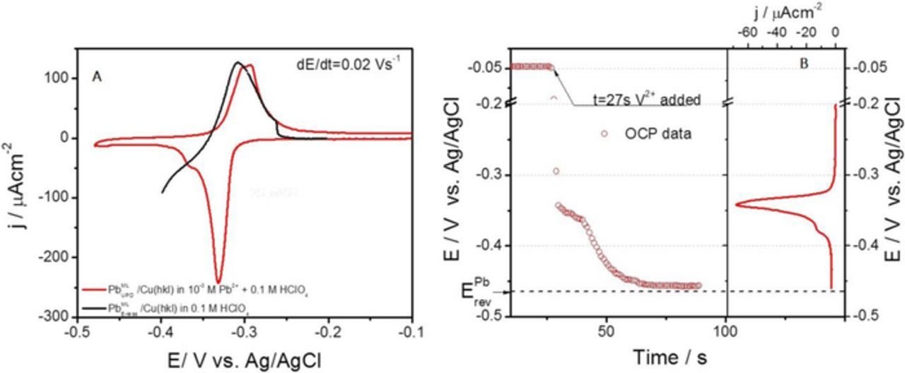
Figure 6. (A) Cyclic voltammetry of the Pb underpotential deposition/stripping process (red line), and linear sweep voltammetry of the e-less Pb monolayer stripping (black line) on/from Cu(hkl) surface. (B) Open circuit transient during e-less Pb ML deposition (red dots) and Pb UPD monolayer stripping (red line) on/from Cu(hkl). Lead reversible potential, EPbrev, is indicated in the graph.
The e-less Co growth on Cu(hkl) is achieved using Ti3+ as reducing agent.24 To illustrate the benefit of Pb ML serving as surfactant during Co growth, prior to the growth experiment, a set of different procedures were implemented in order to clean and reduce the Cu(hkl) surface. This also served to emphasize that the morphology of Co film is a function of the starting Cu(hkl) surface as well as to show the effect of Pb ML presence on Cu(hkl). The results are shown in Figure 7. It is obvious that, depending on the implemented pre-deposition treatment procedure, morphology of the Co thin films differs significantly. In fact, the results render the conclusion that the Co growth mode and surface morphology are critically dependent on the preparation history of the Cu(hkl) sample and condition of the starting Cu(hkl) surface. The SEM image 7A shows the 5 nm thick Co film grown on Cu(hkl) which is reduced by 120 s immersion in 10−3 M borohydride solution, and then subsequently immersed in e-less bath for Co deposition. The morphology of the Co film consists of small 3D Co grains which are partially merged in the continuous layer. Image 7B shows the example morphology of the 5 nm Co film which is deposited on Cu(hkl) after the sample was reduced in forming gas for 900 seconds at 250°C. The reduction of Cu(hkl) with hydrogen gas and higher temperature does yield better starting conditions for Co nucleation on Cu(hkl) and the Co film appears more 2D-like. However, larger and faceted grains are not fully merged and high energy grain boundaries with large number of defects are evident. The image 7C and 7D show the 5 nm Co thin film morphology after the starting Cu(hkl) substrate is reduced in forming gas with 1% of CO for 900 seconds at 250°C. The addition of CO is aimed to protect Cu surface from oxidizing during the sample transfer to the electrochemical cell. Obviously, the CO seems to be beneficial as both Co films are much more continuous and 2D like as compared to the sample shown in image 7B. The sample shown in image 7D is obtained after the Pb ML is e-lessly deposited on freshly reduced Cu(hkl) and then transferred to the solution for e-less Co growth. Although both samples, images 7C and 7D, have 2D morphology, the presence of Pb ML on the Cu surface does affect significantly the outcome of the Co growth. The sample in image 7D has a true 2D outlook, very tight and dense grain boundaries and there are virtually no defects in the film. It is also apparent that the Co grains are bigger than in any of other cases discussed. A simple comparison between the samples in image 7C and 7D undoubtedly illustrates the benefit of the e-lessly deposited Pb ML on Cu(hkl) surface prior to Co growth.
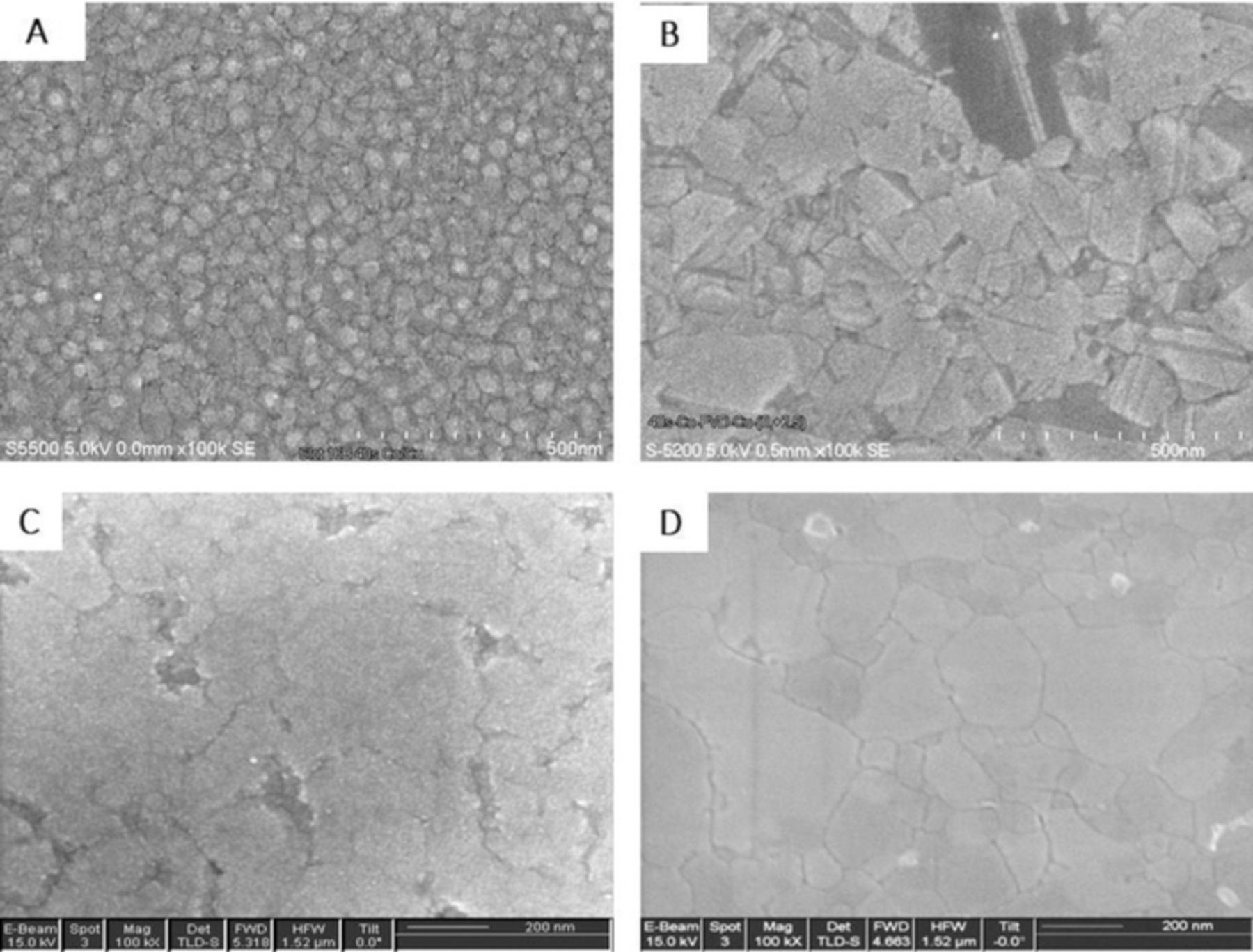
Figure 7. SEM images of the 5 nm Co thin film surface morphology e-lessly deposited on Cu(hkl) for 40 seconds. Cu surface reduced for (A) 120 s in 10−3 M borohydride solution, (B) 900 s at 250°C in forming gas (75% H2+25% N2) (C) 900 s at 250°C in 75% H2+24% N2 +1% CO gas and (D) as in (C) with e-less Pb ML deposited prior to Co e-less deposition.
To further quantify the benefit of e-less Pb ML as a surfactant during the e-less Co thin film growth we have performed the analysis of the AFM data for starting Cu(hkl) surface, and for 5 nm Co thin films on Cu(hkl) produced with and without an e-less Pb ML as surfactant. The results are shown in Figure 8A. One can see that the Co film grown with Pb ML on the Cu surface has the lowest saturation surface width (roughness). It is 2× lower than for the Co film grown without Pb ML and 2.5× lower than the saturation width of the starting Cu surface. Therefore, the AFM data are in a qualitative agreement with the SEM images in Figures 7C and 7D.
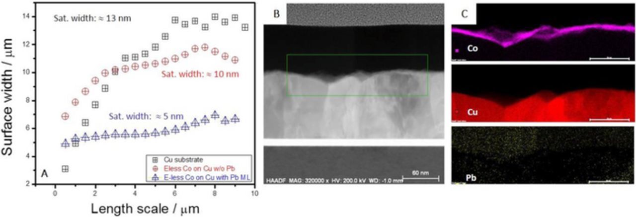
Figure 8. (A) Scaling analysis of AFM images for Cu(hkl), e-less 5 nm Co/Cu(hkl) thin film and e-less 5 nm Co/Cu(hkl) thin film deposited with e-less Pb ML serving as surfactant. (B) High angle annular dark filed transmission electron image of 5 nm Co/Cu(hkl) thin film deposited using e-less Pb ML serving as surfactant (C) Nano EDS map for image in B showing Co, Cu and Pb signal.
The OCP during e-less Co deposition is more negative than the reversible potential of Pb (EsOCP≈ −0.5 V vs. Ag/AgCl) and therefore the e-lessly deposited Pb ML is stable on the surface during the course of the Co growth. Considering that the Pb has lower surface energy than Cu and Co, i.e. γPb < γCu or γCo37,38 from basic thermodynamic arguments,3 one expects that Pb ML should float on top the growing Co surface. However, if the Co deposition is fast enough, it is also possible that the Pb ML gradually becomes trapped in Co film. The thermodynamically unlike scenario is that Pb ML stays at the Co/Cu interface where it is originally deposited. To investigate these possibilities in more detail, we have done the nano-EDS mapping of the TEM cross-section of the Co film deposited on Cu with e-less Pb ML serving as surfactant. The data are shown in Figures 8B and 8C. The rectangle in Figure 8B shows the area of TEM image upon which the nano-EDS analysis is performed. Results indicate that Co surface, Co film and Co/Cu interface are completely free from Pb. Therefore, it is likely that Pb ML remains floating on top of the growing Co during the growth and is eventually washed off during sample cleaning step with DI water.
To further evaluate the benefit of e-less Pb ML as a surfactant we have done magnetic characterization of the Co films. For the thickness regime of 5 nm, the easy magnetic axis for Co is defined by shape anisotropy. The easy magnetic axis is in the plane of the film.39 The in-plane vibrating sample magnetometer (VSM) data for 5 nm Co films grown with and without e-less Pb ML as surfactant are shown in Figure 9A. Mutual comparison of the loops indicates clearly that Co film grown with Pb ML as surfactant shows a higher degree of in-plane magnetic anisotropy. This can be directly linked to its lower defect density, lower stress state and better crystallinity.39
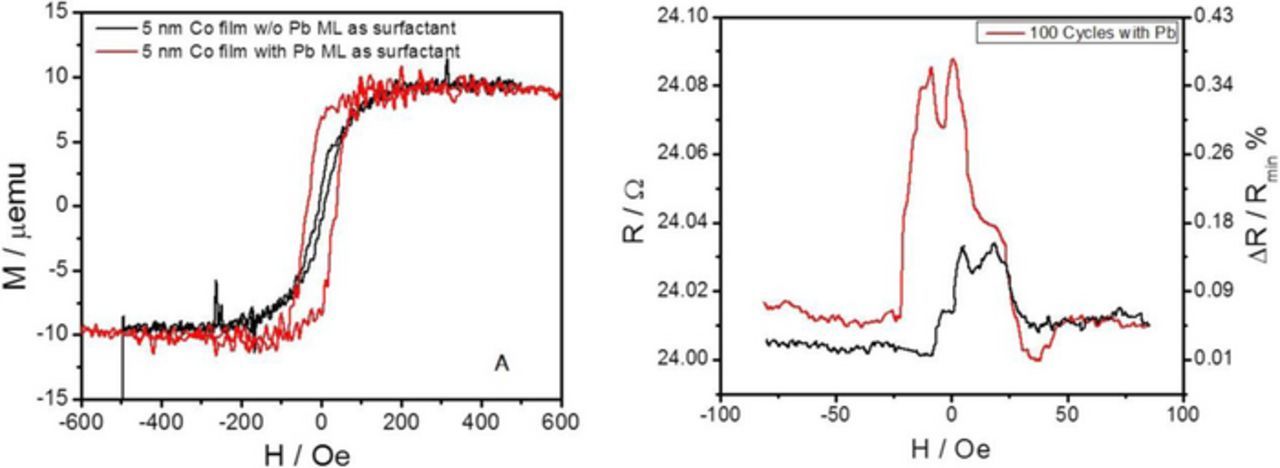
Figure 9. VSM in-pane magnetic loop measurements for 5 nm e-less Co/Cu(hkl) thin film deposited with (red) and without (black) e-less Pb ML as surfactant. (B) Magnetoresistance of e-lessly deposited 100 x Co(0.5 nm)/Cu(2 nm) GMR stack on 2 nm Ru seed using e-less Pb ML as surfactant.
We have also performed an additional experiment to evaluate the effect of the e-less Pb ML as surfactant on the quality of the e-lessly grown Co films. For this purpose, we deposited e-lessly a 100 repetition of the Co(0.5 nm)/Cu(2 nm) bi-layers as a giant magnetoresistance stack (GMR) on 2 nm Ru seed and evaluated it's magnetoresistance in current perpendicular to plane configuration (CPP). Deposition of the GMR stacks was done using our automated set up for e-less atomic layer deposition.40 Deposition of the Co/Cu bi-layer consisted of several e-less deposition and rinsing steps which are part of the repetitive sequence. They are: e-less Cu deposition (1 sec, step 1), the e-less Pb ML deposition (60 sec, step 2) and e-less Co deposition (40 sec, step 3). The magnetoresistance measurements are shown in Figure 9B for positive (red) and negative (dark) magnetic field scan direction. One can see that measured normalized change in resistivity (ΔR/Rmin) values are around 0.3 %. These values are not impressive, nevertheless they do represent the first e-lessly grown GMR stack report. The lack of the magnetic field during the growth of GMR stack resulted that the magnetization orientation of the Co interlayer is not along the common axis (not uniaxial) and thus the positive and negative scan direction show different values of GMR. However, the observation of the GMR grown with Co layers in a presence of Pb ML as surfactant on Cu surface demonstrates that Co layers are highly compact and conformal although nominal thickness is only 0.5 nm. It is certain that the optimization of the solutions design and exposure times for proper layer thickness control is yet to be done, but the results in Figure 9B are encouraging. On the other hand, the e-less GMR stack grown without e-less Pb ML (step 2) did not produce any measureable ΔR/Rmin values. Therefore, the benefit of Pb ML as a surfactant for e-less Co growth is demonstrated once again.
Conclusions
The universality of the Pb ML as the mediator in the electrochemical thin film growth has been demonstrated in two fundamentally different systems and processes. In the first case, the 2D growth of Cu on Ru(0001) has been induced using the Pb UPD ML serving either as a surfactant during potentiostat electrodeposition (SMG), or as a flux mediator during electrodeposition involving continuous potential cycling (DMG). The Pb mediation of the growth process has led to 2D growth by facilitating the Cu step flow (SMG) or by promoting the nucleation stage (DMG). In addition to these two electrodeposition approaches, the 2D Cu growth via SLRR of Pb UPD ML has been demonstrated as well (electroless process). The Pb ML served as a reducing agent for Cu2+ and also as growth mediator and promoter of step flow and nucleation stage. As a second example of the Pb ML mediated growth, the new process for e-less deposition of Pb ML has been demonstrated and used as an enabling phenomenon for Pb ML mediated growth of Co on Cu(hkl). The presence of Pb ML on a starting Cu surface induced the 2D growth of Co thin films in an electroless deposition process. The morphology of the 2D Co films was characterized by smooth and large grains, low defect density and surface width and improved magnetic properties. The presented results and findings should be of broader significance for thin film community as they demonstrate the effectiveness of the Pb ML mediated growth and its ease of implementation. It is likely that other hetero-epitaxial systems could benefit from presented approaches. Our current efforts are directed toward expanding the frontiers of Pb ML mediated growth to other systems and exploring other more environmentally compatible UPD systems and reducing agents which would make application of the discussed mediation approach easier for implementation at the industrial scale.
Acknowledgment
The experimental material is based upon work supported in part by the National Science Foundation under the contract CBET 1605331 and Lam Research Corporation gift grant.
ORCID
S. R. Brankovic 0000-0001-8250-8382