

Abstract
Use and performance criteria of photonic devices increase in various application areas such as information and communication, lighting, and photovoltaics. In many current and future photonic devices, surfaces of a semiconductor crystal are a weak part causing significant photo-electric losses and malfunctions in applications. These surface challenges, many of which arise from material defects at semiconductor surfaces, include signal attenuation in waveguides, light absorption in light emitting diodes, non-radiative recombination of carriers in solar cells, leakage (dark) current of photodiodes, and light reflection at solar cell interfaces for instance. To reduce harmful surface effects, the optical and electrical passivation of devices has been developed for several decades, especially with the methods of semiconductor technology. Because atomic scale control and knowledge of surface-related phenomena have become relevant to increase the performance of different devices, it might be useful to enhance the bridging of surface physics to photonics. Toward that target, we review some evolving research subjects with open questions and possible solutions, which hopefully provide example connecting points between photonic device passivation and surface physics. One question is related to the properties of the wet chemically cleaned semiconductor surfaces which are typically utilized in device manufacturing processes, but which appear to be different from crystalline surfaces studied in ultrahigh vacuum by physicists. In devices, a defective semiconductor surface often lies at an embedded interface formed by a thin metal or insulator film grown on the semiconductor crystal, which makes the measurements of its atomic and electronic structures difficult. To understand these interface properties, it is essential to combine quantum mechanical simulation methods. This review also covers metal-semiconductor interfaces which are included in most photonic devices to transmit electric carriers to the semiconductor structure. Low-resistive and passivated contacts with an ultrathin tunneling barrier are an emergent solution to control electrical losses in photonic devices.
Export citation and abstract BibTeX RIS

Original content from this work may be used under the terms of the Creative Commons Attribution 3.0 license. Any further distribution of this work must maintain attribution to the author(s) and the title of the work, journal citation and DOI.
Recommended by Dr Masud Mansuripur
1. Introduction
Russel Ohl investigated photoconductivity changes in silicon at Bell Labs in the 1940s [1], which can be considered as a starting point for the research and development of semiconductor photodetectors. In 1954, Daryl Chapin, Calvin Fuller and Gerald Pearson demonstrated the first silicon solar cell [2, 3]. They also described three challenges to improve the solar cell performance: (i) large light reflection from the surface, (ii) recombination of electric carriers generated by photons absorbed in the material, and (iii) difficulty to prepare reliable and low-resistance metal contacts to silicon. Since then, scientists and engineers have developed these device properties step by step to meet the ever-increasing need for durable high-efficiency and low-cost Si solar cells. These targets provide a guideline also for this review which strives to strengthen connection between surface physics and photonics, providing a complementary approach to tackle semiconductor surface-induced challenges.
Alongside of huge development of Si microelectronics during the last 80 years [4, 5], various photonic devices based on Si have been also developed, providing synergy between electronics and photonics. For example, silicon photonic circuits are an emergent system studied intensively for different data transfer applications [6–8]. In addition to Si, III–V compound semiconductors such as GaAs, GaN, and InP form the second mature material system of industrial photonic devices. The III–V crystals are nowadays used, particularly, in the devices where the photo-electrical performance of Si does not meet industrial criteria. These devices include for example the light emitting diodes, laser diodes, and infrared photodiodes [9–13].
There are different criteria for optoelectronic devices depending on the applications where a device is used. Such requirements include energy efficiency, high signal sensitivity and speed, intensive light output, and durable operation for instance. Furthermore, from the viewpoint of industrial manufacturing of the devices, available methods should enable scalable, low-cost, and energy-efficient fabrication with a high yield of the fabricated devices in sustainable manner. Thus, the resulting performance of industrial photonic devices is typically a compromise of various factors.
It has been known for a long time that surface areas of semiconductor crystals are a weak part of many photonic devices. The list of solar-cell challenges, reported by Chapin, Fuller and Pearson in 1954 [2, 3], included also different Si-surface induced challenges. Two main functions of semiconductor surfaces are to guide light and electricity in devices. A semiconductor surface in devices is not typically visible or directly in contact with air. In contrast, a semiconductor surface is often hidden below a thin film(s) and hermetic packaging material; i.e. a semiconductor surface lies at an embedded interface between a semiconductor crystal and insulator or metal (figure 1). Still semiconductor surface areas have interacted with various chemical environments during the device manufacturing processes before a final encapsulation. These interactions have changed the semiconductor surface properties, which finally causes different loss mechanisms in the devices.

Figure 1. Examples of photonic device structures. (a) Silicon solar cell, so-called passivated emitter and rear cell (PERC) which includes oxide-silicon and metal-silicon interfaces. Reprinted from Green [45]. Copyright 2015 With permission from Elsevier. (b) Silicon photonic circuit with Si waveguide and some components: Ge photodiode and Si p–n junction modulator. Reproduced from Silicon photonic circuit with Si waveguide and some components: Ge photodiode and Si p–n junction modulator. Figure is taken from Siew et al [7]. CC BY 4.0. (c) III–V compound semiconductor laser diode with two mirrors one of which is coated by Au/Si/SiO2 reflector. Reprinted from Guan et al [46]. Copyright 2016. With permission from Elsevier. (d) Micro-LED of III–V nitrides with sidewall passivation film of SiO2. Reproduced from Wong et al [47]. CC BY 4.0.
Download figure:
Standard image High-resolution imageThus, the surface passivation, which means decreasing of surface-related losses in broad sense, has been investigated intensively from the perspectives of both electronic and photonic devices, in particular, for the industrial semiconductors of group-IV (Si, Ge) and III–V's [e.g. books 14–17]. Indeed this great background knowledge has enabled also photonic device manufacturers to decrease losses and malfunctions.
However, the current and also future photonic devices still suffer from semiconductor surface properties. One reason for the claim is a strong reactivity of most semiconductor surfaces then with environment like with air, chemical solutions, gases in film growth, or metal elements. It is very difficult or impossible to avoid interactions in practice during device manufacturing, leading to the formation of an embedded interface layer between a semiconductor crystal and a thin film. A thickness of the reacted layer is readily larger than 1 nm; i.e. thicker than six atomic layers.
Furthermore, the chemical and structural properties of a reacted interface zone are different from the relatively well-known properties of the bulk materials, which causes changes in the interface electronic structure and finally in devices' photo-electrical performance. The interface changes include the formation of point defects and defect-induced electronic levels or states in the device. To give an example estimation for defect densities, let us consider that an inherent background impurity or defect concentration in a high-quality bulk semiconductor crystal is in the range of 1·1010–1·1014 defects per cm3, which means a planar defect concentration of 5·106–2·109 defects per cm2. For practical semiconductor interfaces, a defect density (Dit) is typically much higher than 1·1011 defects per cm2. The meaning of semiconductor interfaces can be expected to increase further when size or thickness of the functional semiconductor crystals deceases.
To contribute in this technological area, we would encourage the scientists and engineers to consider a complementary edge for approaching the surface challenges, and to enhance collaboration between the communities of photonic devices and surface physics. These two areas have developed rather separately and from different perspectives. Indeed excellent review articles have been previously published about the both subjects: e.g. [18–33] for the semiconductor passivation and [34–44] for the semiconductor surface science.
The surface passivation of devices has been developed mainly with the methods available in semiconductor technology while surface physicists have typically used ultrahigh vacuum (UHV) instruments to refine a well-ordered crystal surface, so-called model system of vacuum-semiconductor interface in chemically inert, non-reactive environment of UHV [e.g. books 48–50]. In contrast, passivated device surfaces often form a solid–solid interface at which the chemical and physical properties of a semiconductor surface have significantly changed due to the surface reactions with other elements, as compared to the clean and crystalline surface. This might lead to confusions if expectations in technology are based on the knowledge obtained from clean and crystalline surfaces in UHV. In other words, the translation of knowledge from surface physics to industry is not necessarily straightforward.
Despite these differences, there are also connecting research items and questions some of which we attempt to review here. Before that, in section 2 we summarize common harmful effects of semiconductor surfaces on optical and electrical behavior of the photonic devices, and in section 3 some fundamental properties of Si, Ge and III–V surfaces are presented. Then we review eight selected topics which hopefully provide a useful platform to share information and to foster productive dialogue between the communities.
The first topic is related to properties of a wet chemically cleaned semiconductor, which can be rather different from the properties of a well-ordered crystal surface in UHV but which are very crucial to the device manufacturing where semiconductor surfaces are cleaned in different chemical solutions several times at various stages of a manufacturing process flow. The second subject is related to the question if it possible to avoid a significant incorporation of oxygen and carbon impurities at the practical semiconductor surfaces. Furthermore, it is often possible to conclude that surface areas cause optical and electrical losses in device operations, which further implies the presence of defect-induced electron levels in the semiconductor band gap. However the questions like which defects cause the gap levels, and from what they originate, are typically much more challenging to answer but are relevant to the efforts to avoid the formation of defect-induced levels in a controlled way. These issues are behind the third and fourth subjects reviewed. The fifth one is related to metal contacts (i.e. metal-semiconductor interfaces) to transmit the electrical current into functional semiconductor parts. There are two main criteria for the passivated contacts: low resistivity and low recombination (or generation) of electric carriers. Then, the surface passivation of semiconductor nanocrystals is considered, and surface challenges of an emergent industrial material, SiC are presented. Finally, surface properties of novel two-dimensional semiconductors are shortly summarized.
2. Effects of semiconductor surfaces on photonic device operations
Semiconductor surfaces, which often lie at the embedded interfaces beneath a thin insulator or metal film, participate in the transmission of light and electricity in the photonic devices. Some general interface challenges, which make the semiconductor surfaces as a weak part of many devices are summarized in this section to motivate the review of specific surface properties and selected subjects in the subsequent sections.
Before these challenges, we present a summary of Si solar cell processing steps to give an example of various treatments, environments, and materials used in practice. The fabrication process of solar cells involves a series of steps, and their details can vary significantly depending on the Si wafer doping and the solar cell structure. The predominant solar cell type in the current industry is passivated emitter and rear cell (PERC). Its structure is presented in figure 1(a), and its processing consists of the following main steps: 1. Substrate preparation: A high-quality Czochralski grown or float-zone silicon ingot with high purity (>99.9999) is diced into wafers using a diamond-coated wire, resulting in surface saw damage and debris. The saw damage can be chemically removed using etching solutions such as Piranha. 2. Front surface texturing: To reduce reflection from the flat surface, as discussed in section 2.1, the substrate is textured using an acidic solution like HF/HNO3 or an alkaline solution like KOH or NaOH, depending on the substrate's crystallinity. Alternative texturing methods include laser texturing, plasma etching, and metal-assisted chemical etching. 3. Formation of p–n junction: the p–n junction is created by introducing the dopants via ion implantation or diffusion at the front surface. In the more common technique of diffusion, wafers are exposed to gas precursors of dopants, either boron or phosphorous. This process is followed by a drive-in annealing process to activate dopants and form a highly doped and crystalline region known as the emitter. 4. Anti-reflection coating (ARC) deposition: Another technique discussed in section 2.1 is the deposition of ARC to further reduce reflection resulted from the difference in refractive indexes of substrate and air at the front surface. The main method for ARC deposition is the plasma-enhanced chemical vapor deposition (PECVD) technique. The selection of ARC material and its thickness are optimized for specific wavelength and substrate material. The commonly used ARC is a Si3N4 film which, with an 80 nm thickness, results in almost 0% reflection at 550 nm. 5. Rear surface electrical passivation: The rear surface is passivated using a dielectric material to reduce recombination losses. The common passivating materials are SiO2 and Al2O3 films. 6. Laser ablation: A laser is employed to create line openings in the ARC layer on the front surface and localized openings on the rear to allow metal contact deposition on the emitter and base sides, respectively. 7. Metallization: The final step is the metallization of front and rear contacts, which can be done using a wide range of materials and techniques. The common method in the industry is screen printing of silver on the front surface and aluminum on the rear surface. This step is followed by a high-temperature firing to form an ohmic contact. Moreover, there are several chemical cleaning steps of surfaces between the aforementioned steps, typically involving so-called standard cleaning 1 and 2 (also known as RCA 1 and 2), which consist of NH3 and HCl, respectively.
2.1. Reduced light transmission into solar cells and photodiodes
When light from the ambient environment interacts with the semiconductor, it may be either reflected or transmitted into the semiconductor. The refractive index is a crucial factor that affects the behavior of light at the interface between two media. For dielectric material with negligible magnetic interactions, the refractive index, n, is related to the dielectric constant (or permittivity),  , of the material with the relation n = 1/2, where is a function of wavelength. In the case of a semiconductor material, such as silicon, the refractive index is significantly higher than that of air or other ambient environments due to higher permittivity [51].
The behavior of light at the interface between two media with different refractive indices is governed by the Fresnel equations, which describe the amount of light that is reflected and transmitted as a function of the angle of incidence and the refractive indices of the two media [51]. The high refractive index difference between semiconductor and air causes a considerable amount of light to reflect back from the surface of the semiconductor, reducing the efficiency of the device.
To reduce reflection for solar cells and photodiodes, antireflection coatings (ARCs) [52–54] and surface texturing techniques [55–61] are designed. By carefully engineering the refractive index of the surface, the reflection can be minimized, allowing more light, particularly in the wavelength range of interest, to pass into the semiconductor material and be absorbed, resulting in higher device performance and new applications.
ARCs consist of dielectric thin films with specific thickness that exploit the interference effects of light [52, 53]. However, a single-layer ARC can only provide nearly zero reflection at a single wavelength and incidence angle. As illustrated in figures 2(a)–(c) [54], increasing the number of layers in the ARCs can lead to achieving almost complete reflection suppression over a wide range of wavelengths, but this also entails a rise in the intricacy of both the design and manufacturing processes (such as figure 2(a)).
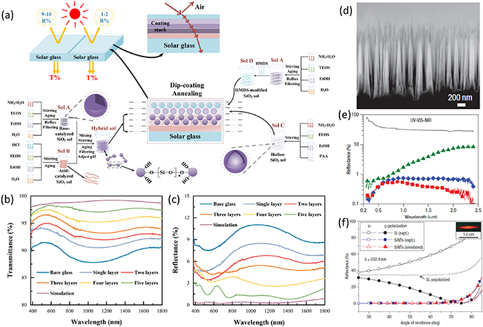
Figure 2. Examples of ARCs and surface texturing techniques. (a) Schematic diagram of the preparatory process of five-layer gradient refractive index broadband ARCs on a glass substrate and the corresponding (b) transmittance and (c) reflectance spectra with different layers. Reprinted from Wu et al [54]. Copyright 2022. With permission from Elsevier. (d) Cross-sectional view of silicon nanotips (SiNTs). (e) Comparison of the specular reflectance from planar Si wafer (solid line) and SiNTs (symbols) for nanotip lengths (L) 1.6 μm (green), 5.5 μm (blue) and 16 μm (red). (f) The reflectance of flat Si wafer and the SiNTs (L = 1.6 μm) as a function of angle of incidence using s- and p-polarized light of 632.8 nm wavelength. Reproduced from Huang et al [59]. With permission from Springer Nature.
Download figure:
Standard image High-resolution imageSurface texturing is the process of modifying the surface of materials to create specific structures, which can reduce reflection across a broad range of wavelengths. Surface texturing can be achieved by several methods, the choice of which depends on the type of material, the desired texture, and the production volume [55–57]. The interaction between the incident light and the surface texture depends on the size of the surface features relative to the incident wavelength. If the size of the surface features is much smaller than the incident wavelength, the surface appears optically smooth for the incident wavelength. However, if the size of the surface features is comparable to the incident wavelength, the surface appears rough, and the reflection is reduced by graded refractive index originated from the graded density profile between the air and the surface. As the size of the surface features are larger than the wavelength, the incident light can be trapped with increased optical path lengths during the multiple reflections between surface textures. Surface texturing also increases the acceptance angles for the incident light to semiconductors, as illustrated in figures 2(d)–(f) [59], which has resulted in a high performance Si-based solar cell [60] and photodiode [61]. In practical applications, minimizing the reflection is often achieved by a combination of surface texturing and ARCs that simultaneously act as surface passivation layers.
An emerging technique of light trapping is the use of plasmonic structures [52, 62–65]. These structures can trap and confine light through the plasmonic resonance effect, which arises from the interaction between the incident light and the free electrons in the metallic/non-metallic nanoparticles or nanoholes. Plasmonic structures can provide broadband and angle-independent light trapping [62–64], making them an attractive option for enhancing the performance of solar cells and photodiodes. Furthermore, plasmonic structures can be integrated with surface texturing and ARCs to create metamaterials with unique optical properties that cannot be achieved with conventional materials [65].
In addition to reducing reflection, spectral converters are another approach used to enhance light absorption in various applications. These converters can absorb light at one wavelength and emit it at another, allowing for better matching of the incident light to the absorption properties of the material. Luminescent downshifters [66] and upconverters [67] are examples of spectral converters that have been widely used to extend the absorption spectrum.
2.2. Light scattering in waveguides
Light waveguides (figure 3) consisting of SiO2/Si cladding-core structure on the silicon-on-insulator (SOI) wafers are used in low-loss optical transceivers for example [6–8, 68–73]. The SiO2/Si interface have a high refraction-index change which is beneficial for the waveguides based on the total internal reflection of light at the interfaces. Furthermore a clean Si crystal is transparent to the telecom wavelengths of 1.3 and 1.6 μm. Obviously good synergy has been obtained here via the development of SOI technology in microelectronics because high crystal quality of Si core with a low density of impurities in the Si/SiO2/Si wafer has decreased the light transmission losses. Yet, interface areas of the Si waveguide stripes on SiO2 cause the optical losses via different phenomena. One loss mechanism arises from the Si interface roughness. The signal attenuation coefficient (dB cm−1) is proportional to the square of roughness, specifically to the square of a standard deviation of the roughness [68, 69]. For low-loss waveguides, it is required very smooth waveguide sidewalls with the roughness less than 1 nm down to an atom layer thickness. Indeed, proper Si surface treatments such as the RCA-based wet chemical cleanining and oxidation of Si waveguide interfaces have been found to decrease the scattering loss [69, 70].

Figure 3. Infrared light absorption in Si waveguide at the SiO2/Si interfaces via defect-induced electron levels in the Si band gap. The signal is further absorbed by electric carriers: electrons in the conduction band and holes in valence band. In figure 1(b), Si waveguide is presented as a part of circuit. Reproduced from Grillanda and Morichetti [72]. CC BY 4.0.
Download figure:
Standard image High-resolution imageIn addition, the SiO2/Si interfaces include point defects (e.g. broken dangling bond and impurities), which cause extra defect-induced electron levels in the Si band gap. The telecom infrared photons that are not able to excite the clean Si crystal through the direct electron transfer over the band gap can be now absorbed via the interface defect levels inside the gap (figure 3). This is one absorption way for the waveguide light. Another loss factor is related to the electrical carriers, electrons and holes. So-called free-carrier absorption is described with the Drude model of the electrical resistance where light is absorbed by the collective oscillation of the electric carriers along the light electric field, causing the resistive loss [71–74]. It is worth noting that the free carrier absorption, which is directly proportional to the density of the carriers, is relevant also to other photonic device components where high carrier concentrations appear, for example, in highly doped to n-type or p-type regions at metal/semiconductor contacts [73, 74].
2.3. Laser mirror damages
Edge emitting laser diodes include both high and low reflective mirror structures fabricated on the cleaved semiconductor (110) sidewalls (figure 1(c)). These lasers suffer from the catastrophic optical mirror damages (COMDs) which limit the device lifetime [75–87]. When the temperature of a diode mirror increases locally (on area of micrometer scale) to a range of 100 °C–200 °C, the COMD phenomenon can occur, during which the mirror temperature increases rapidly even to 600 °C [83, 84]. That causes significant structural degradation leading to the laser malfunction (figure 4).
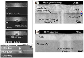
Figure 4. (a)–(c) In-situ thermographic images from 650 nm GaInP laser mirror when catastrophic optical mirror damage (COMD) is occurring (b) in interval of 2.3 ms before (a) and after (c) COMD. (d) Scanning electron image after COMD shows an extrusion. Reproduced from Ziegler et al [84]. With permission from Springer Nature. (e) and (f) Transmission electron microscopy images after two different cleanings of semiconductor facets in diode mirrors: hydrogen (e) and cleaving in ultrahigh vacuum (f), combined with ZnSe passivation film. Reprinted from Boschker et al [86]. CC BY 4.0.
Download figure:
Standard image High-resolution imageReasons for the initial temperature increase at the laser mirrors have been investigated for long. It is widely accepted that defect-induced gap levels at the cleaved diode surfaces play a key role behind the electron-transfer processes that finally lead to the local temperature increase. The band gap defect levels increase carriers' non-radiative recombination which increases the semiconductor temperature. On the other hand, the defect levels increase an opposite electron transfer via thermal generation of the carriers to the conduction band. Furthermore, the gap levels and the free carriers increase the laser light absorption and the resistive heating of the device material. These different electron-transfer processes are expected to increase and sustain each other in the presence of light absorption.
Thus, decreasing a density of the band-gap defect levels at the semiconductor mirror facets is crucial to increase the lasers lifetime. This requires understanding of different III–V(110) surfaces (section 3) because the area of a laser waveguide typically includes a heterostructure of different III–V films including quantum wells. The mirror structure often includes a stack of insulator and/or metal films. Recently it has been shown that cleaving the diode mirror facets in UHV environment followed by in-situ deposition of ZnSe passivation layers before air exposure on the facets increases the device lifetime [86].
2.4. Trade-off between Ohmic and recombination losses at metal-semiconductor interfaces
Most photonic devices contain metal/semiconductor junctions to transmit the circuit current through a semiconductor part or out of it in the case of solar cells and photodiodes (figure 1). These interfaces have been traditionally categorized Ohmic or Schottky contact depending on how the semiconductor electronic bands bend near the interface. The band bending means the presence of an internal electric field (even without an external bias) inside the semiconductor, which originates from the electrons' transfer between a metal and semiconductor to align their Fermi levels according to the Volta contact potential rule. The band bending depends also on the doping type and is different for n-type and p-type crystals. However, at Ohmic interfaces, the band bending is such that semiconductor majority carriers accumulate close to the interface while at Schottky contacts, the majority carriers deplete, are repelled away from the interface [88–90].
Schottky contacts themselves have been utilized as a rectifier and a simple photodetector (e.g. in thermal imaging devices) [91–95] while Ohmic contacts are needed for many devices to transmit the electric current through a device p–n junction structure with a minimized resistance [88, 89, 96, 97]. Two parameters should be minimized in high-quality Ohmic contacts: contact resistivity and carrier recombination (or generation). Toward the first target, the n-type or p-type doping atom density needs to be maximized [98, 99], which on the other hand increases the harmful free-carrier absorption of light (section 2.2). The high doping typically increases also the density of point defects, which is further increased by interactions of metal atoms and a semiconductor. Therefore, the metal contact areas include an increased number of gap levels, which increase carriers' recombination. Thus in many photonic devices, the Ohmic contacts are a compromise between the efforts to increase the doping concentration and to decrease the density of defect levels. The third critical factor is durability of the Ohmic contacts. For example, degradation of the Ohmic contact of p-GaN decreases operation time of ultraviolet LED [100].
Furthermore, an additional factor increases the gap levels at metal contacts: metal-induced gap states (MIGS) which arises from extension of metal wavefunctions into a semiconductor side as shown in figure 5 [96]. To reduce MIGS effects, ultrathin insulator barriers are investigated for passivating the device contacts, which we will return to in section 4.5.

Figure 5. Formation of metal-induced gap states (MIGS) in a semiconductor band gap due to extension of electron wavefunctions from the metal. The interface includes also defect-induced electron levels (blue lines), for example, due to metal atom diffusion into the semiconductor. Reprinted from Robertson and Lin [96] Copyright 2011. With permission from Elsevier.
Download figure:
Standard image High-resolution image2.5. Carrier recombination and generation at insulator-semiconductor interfaces
As presented above, insulator/semiconductor interfaces guide the light propagation in applications. These interfaces also participate in guiding electric current; blocking the current transport into wrong places. For example, the light absorption induced electric carriers should be guided efficiently to the metal contacts in solar cells and photodetectors (figure 1), while in the LED the current transport along the mesa sidewalls should be suppressed to increase the radiative recombination in high-quality bulk quantum wells. The defect levels at insulator/semiconductor interfaces change significantly the carrier recombination and generation [101–103].
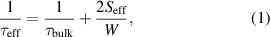
Any defects or impurities at the interface can increase the recombination of electric carriers and deplete minority carriers near the surface. The surface recombination velocity ( ) is often used to specify the recombination at a surface of photonic devices. It can be determined by measuring the effective minority carrier lifetime. Assuming the front and rear surfaces have same properties, the
  can be determined by
where  is the effective carrier lifetime,
  is the carrier lifetime in the bulk, and W is the wafer thickness. Surface passivation can substantially reduce surface recombination by reducing the recombination either by decreasing the defect level density (chemical passivation) and/or electrostatically repelling the electric carriers from the interface by an internal electric field (field-effect passivation). The former passivation is quantified as the interfacial defect density (
 ) while the latter as the fixed charge density (
 ). Recombination can take place either in bulk or at the surface. When surface lifetime limits the effective carrier lifetime compared to the bulk lifetime (
 ), the bulk lifetime can be assumed to be infinite (
 ) and an upper limit for the surface recombination velocity (
 ) can be estimated by
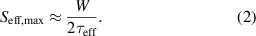
Table 1 in  values for different semiconductor interfaces. The surging demand for photovoltaic devices has spurred significant advancements in surface passivation technology for Si. Notably, the tunnel oxide passivating contact (TOPCon) technology has yielded remarkable outcomes, achieving an exceptionally high carrier lifetime reaching 500 ms (table 1), which translates to
  dropping to less than 0.05 cm s−1. When integrated with industrial processes, these parameters indicate a significant improvement in the energy conversion efficiency of solar panels. Similarly, recent breakthroughs of
  as low as 1.3 cm s−1 on n-type Ge through the optimization of SiO2/Al2O3 passivation layers (table 1) are promising for Ge applications.
In addition to the interface defects, insulator/semiconductor junctions include the band-gap levels also in the insulator side (figure 6), for example, so-called border traps at distances of 1 nm from the interface [104–111]. Thus, the carriers can be lost through the non-radiative recombination at various gap levels. These levels can also cause an additional current channel. Moreover, the gap level also increase the opposite carrier transfer, thermal excitations which cause an increased dark (leakage) current in photodetectors. In many electronic devices based on the metal–oxide–semiconductor stack, the gap levels increase the leakage current through the oxide film as well, which is another type of the leakage; different from the diode dark current. Section 4.4 further describes potential solutions to decrease harmful recombination and generation in devices.
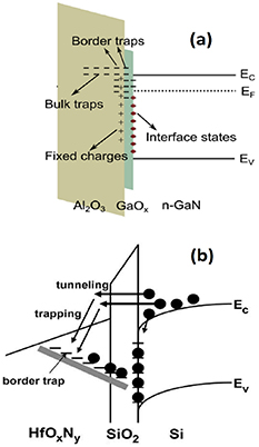
Figure 6. Insulator-semiconductor junctions include various band-gap levels not only at the interface but also inside an insulator at different distances from the interface. Reprinted from Ren et al [110]. Copyright 2018. With permission from Elsevier. (b) Carriers can transfer to different gap levels. Also transfer to opposite directions are possible. External field is applied to the presented junction. @2007 IEEE. Reprinted with permission from Lu et al [111].
Download figure:
Standard image High-resolution image3. Basics of clean and crystalline Si, Ge, and III–V surfaces
For many decades, semiconductor device technology has also stimulated the research of physicochemical properties of semiconductor surfaces, of which atomic scale understanding becomes more and more vital for industrial processes as well. Excellent books [e.g. 48–50, 112] and review articles [e.g. 34–44, 114, 115] are available for the surface science. In this section, we still summarize some fundamental properties of clean semiconductor surfaces, which might be helpful to review the subjects in section 4. For the beginning, we discuss practical methods to prepare a clean surface.
Because semiconductor surfaces typically react strongly with elements of environment, UHV conditions have been widely used to prepare and measure clean semiconductor surfaces. In other environments, a semiconductor surface becomes quickly covered by another material like an oxide or adsorbate layer(s). Based on the kinetic gas theory, the number of atoms or molecules striking a surface per unit area in unit time at room temperature is

where P is the gas pressure in Pa and M is the molecular of atomic weight of the incident particles. For example, at a pressure of 1.5 ‧ 10−4 Pa (=1.5 ‧ 10−6 mbar) of molecular oxygen O2, 4 ‧ 1014 molecules are striking to a clean surface per cm2 per second. If a sticking probability of molecules is unity and molecular adsorption is dissociative, the time required for the adsorption of one layer of O atoms (in relation to the substrate atom density) on the surface is about 1 s. The sticking probability varies between 0 and 1 depending on the elements and adsorbate coverage. Anyhow, UHV conditions (P < 1 ‧ 10−9 mbar) are needed in practice to obtain the understanding of clean surface properties by complementary surface sensitive measurements. Without surface cleaning, a semiconductor surface contains a native oxide film which is typically amorphous and can be several nanometers thick depending on the environment exposure and semiconductor.
There are various methods for preparing a clean semiconductor surface, of which only a few are mentioned here. We return this objective in section 4.1 where it is described effects of the wet chemical cleaning methods which are widely used in device manufacturing processes. It is worth noting that a clean surface does not have a unique definition. In many surface physics studies, a clean surface implies also a crystalline surface. However, this is not the case in more general, and a clean surface can consist of a disordered or amorphous layer on the top of semiconductor crystal.
The widely used surface-science technique to clean a Si surface is so-called rapid high-temperature flashing, where a high direct current (e.g. 10 A) is fed for short time through a small Si piece (e.g. 5 mm × 10 mm slice of Si wafer). Repeating an increase of the Si temperature in UHV several times near 1250 °C removes surface oxides and other impurities. It is critical to minimize the heating time at 1100 °C–1150 °C because stable silicon carbide (SiC) clusters tend to form at this temperature, which can hardly be removed from the surface after SiC formation. The flash heating in UHV provides large atomically smooth terraces on Si, as shown below (figure 8(b)).
This method is mainly used for small Si pieces. Many other semiconductors cannot withstand the high temperatures required to remove natural surface oxides, without melting. Thus, an ion (e.g. argon) bombardment is the common cleaning method for Ge and III–V surfaces. The post-annealing at 300 °C–700 °C in UHV is required to recover a crystalline order of the surface layer(s) after the bombardment that can severely degrade the crystal structure. Because UHV cleaning methods have been develop to optimize the surface smoothness and crystalline degree for justified surface studies, a care is needed to apply the methods for device surfaces. The high temperatures and bombardments can significantly degrade bulk crystal quality causing e.g. metal impurity and doping atom diffusion.
3.1. Some fundamental properties of clean and crystalline Si and Ge surfaces
Most solid surfaces experience structural changes (i.e. reconstruction or relaxation) after the surface cut or formation, as compared to the corresponding bulk plane structure, leading to changes in the surface electronic structure as well. The reconstruction means that a two-dimensional phase transition takes place on the surface, causing atomic rearrangements and a change in the surface lattice compared to the planar bulk lattice. In the relaxation, the surface lattice does not change but the atomic positions in the vertical (surface normal) direction change. The reconstruction trend is especially strong for the semiconductor crystals since their covalent bond orbitals typically have a strong angular dependence. This distinguishes semiconductors from metals, in which the bonds between metal ions are formed by a delocalized electron sea. If a semiconductor surface is produced by cleavage of a crystal in UHV, the atoms located on the surface lose one or more neighboring atoms (figure 7). Thus, the outermost atoms have half-filled dangling bonds, i.e. orbitals occupied with a single electron, in contrast to the bulk bonding orbitals with a pair of electrons. The existence of half-filled dangling bonds leads to a significant increase in the total energy of the cleaved crystal. It is therefore energetically favorable for the crystal to rearrange its atomic structure at the surface to minimize a number of the dangling bonds. Since rigid restrictions are imposed on the angles between localized orbitals in semiconductors, surface rearrangements usually lead to drastic changes in symmetry and unit cell size. Moreover, the rearrangement of surface atoms can involve also deeper atomic layers in addition to the uppermost layer. Ultimately, the equilibrium ground-state (i.e. minimum energy) structure is governed by a delicate balance of the energy gain from the elimination of dangling bonds and the energy cost caused by introduced lattice strain in a modified surface layer. Also, the changes in atomic surrounding require typically the modification of electrons' distribution which can cause an additional Coulombic interactions between charged structural elements.
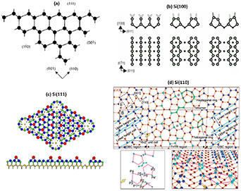
Figure 7. (a) Different low Miller index surfaces of the cubic diamond crystal structure. At the cut (111) and (110) faces, each surface atom has one broken bond while at (100) each atom has two broken bonds. Reprinted with permission from Duke [37]. Copyright 1996 American Chemical Society. (b) Left: atomic structure of bulk-terminated Si(100)(1 × 1); middle: reconstructed Si(100)(2 × 1) with symmetric dimers; right: with asymmetric tilted dimers. (c) Atomic model for Si(111)(7 × 7) surface. Reproduced from Mönch [112]. (d) Atomic model for Si(110)(16x2). With permission from Springer Nature. Reproduced from Yamasaki et al [113]. @ IOP Publishing. All Rights Reserved.
Download figure:
Standard image High-resolution imageThe most common building blocks of the reconstruction on Si and Ge surfaces are dimers and adatoms. The number of broken dangling bonds varies depending on the crystallographic direction of a cleavage plane defined by the Miller indexes (figure 7). On the bulk-plane terminated (111) and (110) faces, there is one dangling bond per the surface atom, while on the (100) surface, each atom has two dangling bonds if no reconstruction occurs.
Thus, it is natural that pairing of the surface atoms and formation of new bonds occur on the Si(100) surface to reduce the number of dangling bonds to half, lowering the material total energy significantly. The paired atoms, dimers, form linear rows and the (2 × 1) unit cell according to the Wood notation where the unit cell length is doubled along one primitive vector direction, as compared to the (1 × 1) bulk plane lattice. If no further structural change occurred, the dimer atoms would be equivalent and have one partly occupied dangling bond per atom. Such degeneracy causes Jahn–Teller distortion where the dimers spontaneously deform lowering their symmetry, as shown in figure 7(b). This leads to an additional decrease of energy. The Si dimer axis is tilted by 18 degree to the (100) surface plane leading to so-called buckled dimers [120]. This means that the Si dimer atoms lie at inequivalent positions, accompanied by electron charge transfer between the dimer-up and dimer-down atoms. Two orientations of the asymmetric dimers are possible, one tilt to the left and the other to the right. At room temperature or higher, rapid fluctuations between the two configurations (so-called flip motion) [121, 122] can occur for dimers continuously such that the dimer tilting does not necessarily appear in the measurement at room temperature, for example, when the surface is probed by scanning tunneling microscopy (STM) or electron diffraction (figures 8(a)–(c)). However, the asymmetric dimers provide a signal when the surface is probed by a fast measurement of the photoelectron spectroscopy that gives a 'snapshot' of tilted dimer configuration [117, 119]. The Si 2p core-level spectrum of Si(100)(2 × 1) surface shows two components: one related to the dimer-up (Su) and the other related to dimer-down (Sd) atoms with the binding-energy separation of 0.5 eV as exemplified in figure 8(d).

Figure 8. (a) Low energy electron diffraction (LEED) pattern shows that the Si(100) surface consists of two domains of (2 × 1) and (1 × 2) where dimer rows are along perpendicular directions in the neighboring terraces. (b) STM image from the flash-heat cleaned Si(100) shows large atomically smooth terraces. (c) Zoomed STM image at room temperature shows dimer rows of one domain without resolving different dimer atoms. (d) Synchrotron XPS Si2p spectrum from Si(100)(2 × 1) + (1 × 2) at room temperature shows two extra components Su and Sd from dimer-up and -down atoms in addition to the bulk crystal component B. (e) Scanning tunneling spectroscopy curve shows that a surface band gap (i.e. voltage range where differentiated intensity is zero) is approximately half of the bulk gap at Si(100)(2 × 1) + (1 × 2). Reprinted with permission from Rad et al [116]. Copyright 2020 American Chemical Society. (f) Calculated band structure shows that the dimer-related bands decrease the band gap at the surface. Charge density contours show that electron density is enriched around the top dimer atoms. Reprinted figure with permission from Pehlke and Scheffler [117]. Copyright 1993 by the American Physical Society. (g) Hydrogen–Si bonding removes dangling bonds, and the formed H-Si bond levels lie outside of the band gap. Reprinted from Robertson et al [118]. With the permission of AIP Publishing. (h) Low-temperature STM image reveals different dimer atoms because their flip motion is decreased at 40 K. Dimer down atoms are imaged when electrons tunnel toward the Si surface. Reprinted figure with permission from Ono et al [119]. Copyright 2003 by the American Physical Society.
Download figure:
Standard image High-resolution imageAt low temperatures (<200 K), the flip motion of dimers slows down, which makes one of two tilted configurations frozen [122]. Moreover, dimers in adjacent rows are oriented in opposite directions, leading to c(4 × 2) and (2 × 2) unit cells (figure 8(h)). Similar structural changes are observed for the Ge(100) surface, and the (2 × 1), c(4 × 2), and (2 × 2) reconstructions form due to dimerization in the first layer of Ge atoms, depending on the temperature [123]. For instance, the tilting angle of Ge dimers (19 degree) is very similar to that of Si dimers [124].
Since the tilted dimer on the Si(100) and Ge(100) surfaces possess one fully occupied dangling bond and one completely empty dangling bond, a semiconducting electronic structure with a surface band gap is formed (figure 8(f)). For the Si(100) surface, a dominant feature in the valence band edge is a surface state Dup associated with the dangling-bond orbital of the dimer-up Si atoms [125]. Likewise, the dominant feature above the Fermi level is a surface state Ddown associated with the dangling-bond orbital of the dimer-down Si atoms. Thus, the band gap of approximately of 0.5 eV (i.e. half of the bulk gap) at clean Si(100) is determined by the occupied and empty dangling-bond levels. At the Ge(100) surface, the electronic properties are complicated by a bulk contribution which is interconnected to the surface lattice via a surface resonance [126–129]. The Ge(100) surface resonance is one probable reason for that the n-type Ge(100) has strong Fermi level pinning at 0.1 eV above the valence band maximum [129, 130].
The Si(111) and Ge(111) surfaces, of which atom densities of 7.84 ‧ 1014 and 7.22 ‧ 1014 cm−2, respectively, are higher than 6.78 ‧ 1014 cm−2 of Si(100) and 6.24 ‧ 1014 cm−2 of Ge(100), exhibit even a greater variety of reconstructions. The specific atomic structure depends on the method used in the preparation of clean surface. For example, the Si(111) surface cleaved in UHV at liquid nitrogen temperature (∼100 K) exhibits the (2 × 1) reconstruction. At 500–700 K it changes to the (7 × 7) reconstruction (figure 7). This phase transition is irreversible, i.e. the (7 × 7) structure persists even after lowering the temperature. At a higher temperature (∼1170 K) the (7 × 7) reconstruction transforms to another phase which is so-called high-temperature (1 × 1) structure. This phase transition is of order-disorder type and has a reversible character, i.e. lowering the temperature leads to the restoration of energetically stable (7 × 7) below 1170 K. It includes 12 atoms in the adatom layer, 42 atoms in the rest-atom layer, and 48 atoms in the layer containing the stacking fault [131]. Counting the atoms amount in the adatom and rest-atom layers, one can find that the (7 × 7) structure needs extra four Si atoms compared to the non-reconstructed Si(111)(1 × 1) surface with the bulk-like termination. From the energetic viewpoint, the benefit of (7 × 7) reconstruction is obvious, because it allows one to reduce the number of dangling bonds by more than two and half times, and thus, the Si(111)(7 × 7) is very stable. In contrast, the Ge(111) shows the c(2 × 8) reconstruction that includes adatoms and rest-atoms. The most detailed information about the electronic structures of Si(111) and Ge(111) reconstructions has been obtained for the (7 × 7) structure [132–134]. They include occupied and empty levels which are localized on the adatoms, the rest-atoms, and the adatom backbonds. The surface band contributed by the occupied dangling bonds of adatoms crosses the Fermi level (i.e. a metallic band structure), leading to Fermi level pinning at 0.7 eV above the valence band maximum for the both n-type and p-type Si(111) samples. Thus the surface work function is independent of the type and doping level of the Si(111)(7 × 7) surface [135].
The atomic structure on the (110) surfaces of Si and Ge is rather complicated and less understood still. When the Si(110) surface is annealed at 1200 °C, it exhibits a large (16 × 2) reconstruction [113, 138, 139]. The building blocks of this structure (figure 7(d)) are a buckled tetramer, heptagonal rings, and a tetragonal ring.
3.2. Some fundamental properties of clean III–V surfaces
In contrast to Si(110) and Ge(110), III–V(110) surfaces are well understood (figure 9), and have provided a well-defined template for surface investigations during decades because clean III–V(110) surfaces can be readily obtained by cleaving cubic III–V crystals. It is worth noting that the cleaved III–V(110) surfaces have been used in the laser diode mirrors. III–V(110) surfaces are an exception because they do not typically reconstruct but have the (1 × 1) bulk-plane lattice according to the Wood definition. However, the surface relaxation occurs at III–V(110) together with electron transfer from the group-III dangling bond to group-V one. The resulting relaxed III–V(110) surface is semiconducting (or insulating) with a clear band gap of which size equals to the bulk band gap (figure 10). In other words, a clean III–V(110) surface does not cause extra electron levels in the middle of the bulk band gap, in contrast to Si(100)(2 × 1) or Si(111)(7 × 7). In fact, the band gap without surface-related electron levels is a rather common property among clean III–V surfaces where the group-V dangling bonds become filled by electrons while group-III dangling bonds are empty [140–144]. In contrast, intrinsic point defects like As substitutional in Ga site (AsGa) cause the midgap levels in the clean surfaces [144].
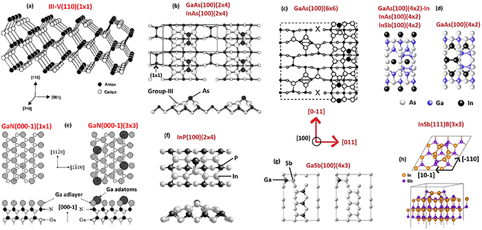
Figure 9. Atomic models for selected III–V compound semiconductor surfaces. (a) III–V(110) surfaces are used for example in laser diode mirrors and can be readily obtained by cleaving the cubic crystal. III–V(110) surfaces do not typically reconstruct but relax. Reprinted with permission from Duke [37]. Copyright 1996 American Chemical Society. (b)–(d) III-As(100) surface reconstructions with decreasing the As amount at the surface. Reprinted from Laukkanen et al [136]. With the permission of AIP Publishing. (e) Surfaces of hexagonal wurtzite GaN crystals can contain extra layers of Ga which form a reconstruction. Reprinted from Smith et al [137]. With the permission of AIP Publishing.
Download figure:
Standard image High-resolution image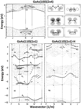
Figure 10. Top: Electronic band structure for GaAs(100)(2 × 4) where solid lines are surface-induced levels. The corresponding orbitals that contribute to the surface bands are also shown. For example the V1 band is contributed by the top layer As dimer dangling bond and C1 arises from the empty second-layer Ga dangling bonds (figure 9(b)). Reprinted figure with permission from Schmidt and Bechstedt [143]. Copyright 1996 by the American Physical Society. Bottom: As and Ga dangling bonds cause electron levels near valence-band maximum and conduction band minimum respectively. When hydrogen atoms are bonded to the dangling bonds, the resulting electron levels move away from the band edges. Black dots mark surface related bands. Pulci et al [141]. John Wiley & Sons.
Download figure:
Standard image High-resolution imageMany clean and crystalline III–V(100) and III–V(111) surfaces undergo strong structural rearrangements (figure 9), and the resulting reconstructions own large unit cells such as (2 × 4) or (6 × 6) or (4 × 2) [145–150]. The same reconstruction principles as for Si and Ge determine largely the structural changes at III–V surfaces also. The III–V reconstructions often extend to a depth of several atomic layers, exposing also the second and third atomic layers, as shown in figure 9. The strongly rearranged III–V(100) surfaces can be in fact expected to cause atomic scale non-uniformity at the interfaces grown on the top of the reconstruction. Thus, a proper adsorbate layer on a clean semiconductor surface might decrease the structural changes at the semiconductor side via the formation of smaller adsorbate-induced unit cell [151–153], and improve atomic-scale smoothness at the interfaces.
Wurtzite III–V nitride surfaces (figure 9(e)) such as GaN(0001) and AlGaN(0001) are an exception among semiconductor surfaces because their reconstructions are typically atomically smooth, which can be understood with strong nitrogen bonds which have partial ionic nature, which hinders the atomic rearrangement [137, 154–159]. In contrast, extra Ga layers have been found to form smooth islands with superstructures. Another peculiar property of III-N nitrides is that they exhibit a surface diffraction pattern without any surface cleaning even after a long air exposure of several months. Strong nitrogen bonds of course decrease the oxygen incorporation into the nitride surfaces but it appears also that the III–V nitride surfaces can accommodate oxygen atoms keeping crystalline nature in different way as compared to many other semiconductor surfaces [156–158].
4. Connecting issues between photonic device interface passivation and surface physics
In this section we present selected research subjects which are relevant to developing the passivation of photonic devices. Strong background knowledge has been previously obtained for the subjects but each of them includes also open issues whose understanding might be progressed via enhanced collaboration between photonics and surface physics people.
4.1. What kind of properties does wet-chemically cleaned surfaces have?
Properties of wet-chemically treated Si, Ge, and III–V surfaces have attracted great interest for several decades because these surfaces are predominantly utilized in industrial processes [e.g. 160–180]. Thus, the semiconductor wet chemistry can be considered a very established area but on the other hand, it is also developed continuously toward sustainable solutions, which for example decrease consumption of chemicals. An obvious difference between the wet chemistry methods and UHV methods (section 3) is the environment of atmospheric pressures during the cleaning and transfer of samples.
Si crystals with the (111) surface orientation appear to be a surprising exception among the semiconductor surfaces because a very high-quality Si(111) surface structure has been observed in STM (figure 11) after a pure wet chemical treatment [169, 171]: Without any additional preparation, a proper F-containing wet etching provides large-scale smooth terraces with atomic scale ordering for hydrogen-terminated Si(111). In the optimized chemical treatment, 1.0% ammonium sulfite was included in the 40% NH4F etching solution for removing dissolved oxygen and for preparing atomically smooth Si(111) [171].
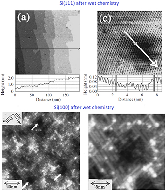
Figure 11. Scanning-tunneling microscopy (STM) images reveal significant differences between Si(111) and Si(100) after wet chemistry. Reproduced from Kato et al [171]. @ IOP Publishing. All rights reserved. Reprinted from Endo et al [167]. With the permission of AIP Publishing.
Download figure:
Standard image High-resolution imageIt is still surprising that Si(100) behaves quite differently from Si(111) concerning the wet chemistry effects. Namely, wet chemically treated Si(100) surfaces have been more rough without large atomically smooth terraces (figure 11). In contrast, different facets are typically formed on wet chemically etched Si(100) surfaces [166, 167, 170]. This difference is consistent with surface-recombination velocity measurements performed in situ during the immersion of Si(100) and Si(111) pieces in a HF-containing solution: Si(111) causes lower recombination velocity than Si(100) [161]. The peculiar behavior of Si(111) can be understood with the surface energetics: energy of the relaxed Si(111)(1 × 1) structure is smaller than that for Si(100)(1 × 1) [172].
If this energy is a significant factor behind the formation of atomically smooth etched terraces on Si(111), then a proper etching of another plane of Si(110) can be expected to produce large terraces more easily than on Si(100). That has not been evidenced by STM so far according to our knowledge. However it can be expected that significance of the wet chemical treatments of Si(110) increases because in many nanocrystals, the (110) planes are exposed and require the passivation. Furthermore, on the basis of the surface energy comparison, it might be speculated that a Si–Si dimer structure during a wet chemical treatment would enhance the terrace formation. However, in-situ STM measurements of Si(111) in NaOH solution [164] suggest that no dimer reconstruction occurs on the surface during the etching.
We would like to emphasize that STM measurements [166, 167, 169–171] have been the key to realize the exceptional properties of Si(111) because the surface diffraction methods (i.e. LEED and RHEED) and x-ray photoelectron spectroscopy (XPS) are not sensitive to local defects. Indeed it is known that STM measurements often reveal realistic surface quality.
Measurements of wet chemically treated III–V and Ge surfaces [174–179] also support that Si(111) is an unusual case because the post heating in UHV is typically needed to increase a crystalline order and the formation of atomically smooth terraces on the etched surfaces. Another difference between Si and III–V is that Si surfaces have typically hydrogen termination after the wet chemistry while III–V surfaces become enriched by group-V element in chemical treatments. Extra group-V adsorbates can be removed at relative low temperatures in UHV [174–178]. For example, extra arsenic from GaAs at around 350 °C. However, recently it has been reported a surprising wet-chemically induced InP(100)c(2 × 2) surface which resembles atomically smooth Si(111), and which is expected to be hydrogen terminated after a proper HCl immersion [179].
Indeed, HCl-based etching solutions have been found to provide smoother surfaces for III–V and Ge, as compared to the F-containing wet chemistry [174–180]. For Ge, both NH4OH- and HCl-based treatments have been used successfully [180]. However, atomically smooth terraces, similar to those of Si(111), have not been reported so far in STM measurements of purely wet-chemical treated Ge surfaces. As mentioned above, the post heating in UHV conditions after a wet chemical treatment has been used particularly for III–V and Ge to obtain atomically smooth large-scale terraces. The UHV post heating also enhances smoothness of Si(100) as shown in figure 12.
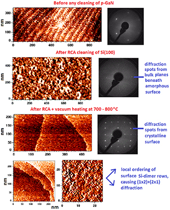
Figure 12. Top: STM image from the p-GaN surface with native oxide before any surface cleaning shows a terrace-step structure and clear (1 × 1) LEED. In contrast, no large-scale atomically smooth terrace is found on Si(100) after the RCA wet chemical treatment with a final HF dip. LEED pattern from this surface shows (1 × 1) spots which arise from the bulk crystal planes beneath the topmost layer(s). Post heating of this surface in UHV around 700 °C–800 °C provides large scale terraces. LEED changes as well to the (2 × 1) + (1 × 2) pattern that appears to arise from local dimer structures seen in zoomed STM image.
Download figure:
Standard image High-resolution imageAfter a wet chemical treatment, a semiconductor surface contains carbon contamination, of which amount can be decreased by low-temperature (<450 °C) heating in UHV. Such incorporation of carbon at the surfaces is expected from the energetical viewpoint [181]. For example, the molecular bond strength of Si–C is similar to Si–H bond strength (360 kJ mol−1). Furthermore, the Si–O bond strength of 450 kJ mol−1 indicates the presence of oxygen incorporation although the H-termination of Si surfaces decreases O incorporation rate.
Theoretical simulations [182–184] for incorporation of carbon, hydrogen, and oxygen atoms into semiconductor surfaces in different chemical solutions and background gases would be helpful to understand the surface properties and their changes during the etching and the sample transfer to a next process step. Finally, GaN surfaces appear to be an exception among all semiconductor surfaces because smooth terraces can be observed even without any treatment (figure 12), which probably arises from the strong Ga–N bonding. Such untreated GaN surfaces still contain oxygen and carbon atoms which are incorporated into GaN without destroying the surface crystal structure completely.
To recapitulate, understanding of the specific properties of Si(111) and InP(100) in comparison to the other surfaces like Ge(111) and GaAs(100) is expected to contribute to development of the methods to decrease the surface roughness and atomic scale disorder. A clean semiconductor surface is not necessarily crystalline. STM characterization is expected to be useful in optimizing a wet chemical recipe which provides a clean and highly crystalline starting surface for the next device processing step.
4.2. Is it possible to avoid the incorporation of significant amount of oxygen and carbon impurities into semiconductor surfaces?
In this section, we do not attempt to make a review on the semiconductor oxidation phenomenon. Excellent books and articles have been previously published about this subject [e.g. 14–17, 185–188]. It is accepted that for an oxidized semiconductor layer thicker than 4 nm, the Deal–Grove model where oxygen diffuses through the oxide film to the oxide/semiconductor interface and oxide growth occurs at the interface, describes the semiconductor oxidation, but the initial states of semiconductor oxidation are expected to be more complex [185–188].
Understanding of these issues is relevant to develop photonic devices because it is not possible to avoid the incorporation of oxygen atoms at practical semiconductor surfaces [e.g. 136, 189, 190]. This subject might be still controversial because sometimes it is described that it is possible to avoid the incorporation of a significant amount of oxygen (or carbon) atoms. Then a relevant question is what is a non-significant density of oxygen atoms because every defect can increase degradation. Second, which characterization method(s) is really sensitive enough to measure a density of oxygen atoms of 1‧1010 cm−2 or lower, which means approximately one impurity per 100 000 host surface atoms or less. Toward that, XPS which is a really element sensitive method has been widely used to determine of a surface chemical composition in non-destructive manner. However, the resolution of XPS is around 0.5–1 atomic % (∼1012–1013 atoms cm−2), which is essential to take into account when making conclusions about non-significant amount of surface impurities [191–193]. Here STM measurements can be useful to reveal potential defect structures with a low and local density. It is still worth noting that oxygen-semiconductor bonds do not necessarily cause the band-gap defect levels directly. In contrast, oxygen incorporation often increases a disorder and, thus a point-defect density (e.g. broken dangling bonds) [194, 195].
Electrical measurements belong to the most defect sensitive probes even if they are not element sensitive. The microelectronic community has utilized capacitance–voltage (C–V) measurements of metal–insulator–semiconductor (MOS) capacitors to understand the interface-defect-induced electron levels [e.g. 196–198, 105, 106]. With the conventional MOS C–V methods, a care is needed to compare different device models in determining exact values of defect densities for comparison. Alongside conventional MOS C–V, also a non-invasive contactless technique called corona oxide characterization of semiconductors (COCOSs) [199, 200] has been developed. This method is based on measuring the surface contact potential via Kelvin probe, and allows to characterize the interface without the need for metal electrodes. The sensitivity of these two C–V techniques is based on a strong effect of defect-induced levels on carrier transport properties close to the semiconductor interfaces.
One argument for that why it is impossible to avoid oxygen atom incorporation into photonic device surfaces is the exothermic nature of oxidation; the formation of oxygen bonds clearly decreases the total (inner) energy of a semiconductor system [201]. Although the H-termination of Si surfaces decreases the oxidation rate, the incorporation of oxygen atoms into Si is expected to start immediately in O-containing environment because the Si-O bond is stronger than Si–H. Furthermore, it is very difficult to avoid the contact of a semiconductor with oxygen-containing environment. As presented in section 3, the vacuum-technology principles describe how a solid surface becomes covered by one adsorbate layer in one second, when the environmental pressure around a solid is as low as 1‧10−6 mbar [202]. If the background pressure is 1‧10−9 mbar, it takes 1000 s for one monolayer adsorption. Thus, a cleaned semiconductor surface becomes readily oxidized unintentionally due to the residual gas conditions which appear for example during the sample transfer to a film-growth instrument. Moreover, the growth conditions for insulating films are very oxygen rich, and interdiffusion of elements across an oxide/semiconductor interface readily increases oxygen incorporation into the semiconductor.
Incorporation of carbon atoms is also expected to occur although the bond strength between adsorbed carbon and a semiconductor element is typically weaker than that of oxygen bonding. This difference is also reflected in the UHV heating effect that the carbon XPS signal decreases in contrast to the oxygen one [116].
The surface reactions after the wet chemistry affect properties of the resulting interface although a high-quality SiO2 film will be grown by the thermal oxidation of Si [61, 203–209]. The high-temperature (>700 °C) thermal oxidation is not possible even for all Si device interfaces. Therefore, low-temperature solution-based wet-chemical oxidation of Si has been developed to prepare an ultrathin SiO2 passivation layer [210, 211]. Indeed, this approach allows to control oxygen incorporation into the interfaces, which would occur anyway at some stage(s) after the wet chemical cleaning. This subject is returned in section 4.4. Furthermore, the oxygen and carbon incorporation can be affected by other elements. Wet chemical nitridation, which provides relatively strong N bonds with III–V surface elements, has been used successfully for the surface passivation [212–214].
To recapitulate, because it is not possible to avoid oxygen and carbon incorporation into practical device interfaces, it might be useful to address the question if the structure of impurity-containing semiconductor surfaces can be modified such that they cause minimized losses [215]. This idea has been also supported by theoretical calculations which show, for example, that a proper oxygen rich GaAs surface provides the HfO2/GaAs interface without the band gap levels [216].
The properties of a clean starting surface, in particular the atomic level smoothness is known to affect the structure of oxide-Si interface and to increase its crystalline order [217–219]. An increased crystalline degree naturally decreases the point defect density. However, it is not an easy task to prepare the atomically smooth starting surface with wet chemical treatments for semiconductors generally, as discussed in section 4.1. For Si(100), depositing thin epitaxial Si layers has been found to be a potential method [217–219].
4.3. Which interface defects do cause extra electron levels in the band gap?
After decades of research, it is nowadays widely accepted that the Si dangling bond, caused by missing of neighboring atom, is the main defect type at SiO2/Si interfaces [e.g. 15, 16, 220–226]. In this defect structure, the Si atom with the dangling bond does not reach four bonds with neighboring Si or O atoms. It is also established that the SiO2/Si interface is not atomically sharp typically. In contrast, the interface layer is extended or diffused at least when the high temperature thermal oxidation of Si is used to grow SiO2 and when the oxygen diffusion toward Si is strongly enhanced (figure 13). It means that the number of oxygen bonds per Si atom increases from one (i.e. Si1+ oxidation state) to four (i.e. Si4+ oxidation state) toward the topmost SiO2. Also very sharp interface models have been developed for SiO2/Si interfaces [217–219], which probably describe low temperature SiO2/Si structures (e.g. wet chemically grown) better than the diffused interface model.

Figure 13. Top: band gap as a function of the distance over the SiO2/Si interface, showing a transition region where the number of oxygen bonds per Si atom varies between Si1+ and Si4+ oxidation states. Middle: atomic models for the SiO2/Si interface with a missing Si atom (i.e. vacancy) at different distances from SiO2. Three-fold bonded Si(1) atom has a dangling bond. Bottom: positions of different dangling-bond induced electron levels in relation to the Si band gap. Reproduced from Li et al [226]. Copyright 2019, with permission from Elsevier.
Download figure:
Standard image High-resolution imageThe dangling bond structures are often called Pb defect which has a variation in the bonding structure depending on the number of oxygen bonds nearby the three-fold bonded Si atom. Understanding of the positions of different defect-induced electron levels in relation to the Si band gap has significantly improved via development of detailed computational physics methods because it is very difficult to measure experimentally the defect level position around the band gap with an atomic identification of the defect structure. Indeed theoretical calculations [e.g. 221, 223, 226] have confirmed that the Pb defects with dangling bond cause extra electron levels in Si band gap (figure 13). It might be still surprising that the density of these Pb-induced levels is often higher than 1‧1012 cm−2eV−1, if the interface is not specifically passivated by hydrogen [224], because SiO2/Si has been considered an unusually high-quality exception among semiconductor interfaces. On the other hand, SiO2/Si is the junction with an amorphous material, and the Si oxidation increases the structural disorder which naturally leads to the formation of point defects.
Structural disorder starts already at initial stages of the Si oxidation [15, 186, 188, 190, 195] where a part of Si atoms also detach and diffuse from sub-surface layers toward the top surface. In other words, Si-vacancy formation in the subsurface is an energetically favored process when the oxidation of Si surface starts [227]. There are also indications that it is possible to increase a crystalline degree of the oxidized Si surfaces [116, 228]. However, in addition to the vacancy-induced point defects (Pb), it is also relevant to consider the electron level distribution in the sub-oxide phases of SiOx because a change in the amount of oxygen can cause an unexpected variation in the electronic structure of SiOx [194]. A similar variation in the electronic structure for different oxide phases has been also found for III–V's [229]. Significance of these issues can be expected to increase in the applications where thin or ultrathin oxide layers are a part of the device structure.
Computational simulations have also improved our understanding of the probable defects causing the band-gap levels at III–V surfaces [e.g. 118, 230–232]. Group-V and -III dangling bonds as well as group-V dimers are the most likely defect structures causing extra electron levels around the band gap (figure 14). Furthermore at InP interfaces, the bonding configurations where P atoms have one or two oxygen bonds (i.e. low oxidation states of P) cause the band gap levels [233]. For III–N nitride surfaces, also carbon impurities have been considered as one dominant defect type [234, 235] but the nitride surfaces are not yet understood as well as other III–V surfaces. Similarly the SiC surfaces need future studies to establish the most probable defects, which include C–C bonding [236–238] even if C–C bond signal is not clear in XPS, but here it is worth to remind the limited XPS resolution and compare it to an expected C–C density.
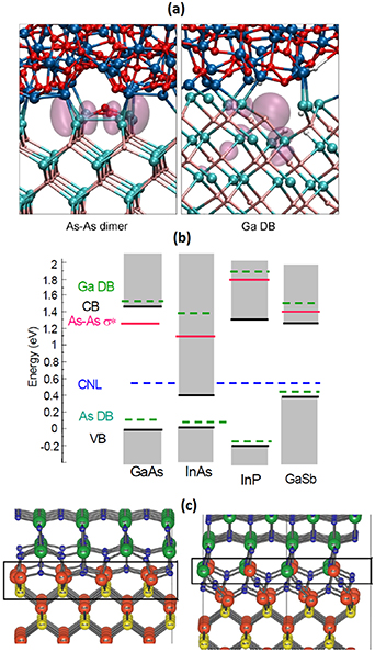
Figure 14. (a) Two potential defect structures at GaAs interface: As–As dimer and Ga dangling bond with charge density contours for electron levels around the band gap. Top film is Al2O3. Reprinted from Miceli and Pasquarello [232]. Copyright 2014, with permission from Elsevier. (b) Probable band gap levels for different III–V's: group-V or group-III dangling bonds (DB) and V–V dimers. Reprinted from Robertson et al [118]. With the permission of AIP Publishing. (c) Two energetically stable atomic models for HfO2/GaAs interface with an oxidized Ga-rich GaAs surface. These structures with a Ga2O3 type interface layer provide defect-level free GaAs band gap. Reproduced from Lahti et al [216]. CC BY 4.0.
Download figure:
Standard image High-resolution imageIn contrast to Si, the native oxides of III–V and SiC are not typically high enough quality for the insulator-film purposes. Therefore, the insulator films (e.g. SiO2, SiN, Al2O3 and HfO2) have been grown by other methods such as CVD and atomic layer deposition (ALD) for insulator/III–V junctions. Still these interfaces include an intermediate layer of oxidized III–V or SiC, which might be useful to include in theoretical models to predict the properties of these interfaces. Recent studies have presented energetically favored structures for oxidized GaAs(100) and InP(100) surfaces [216, 233], which provide a realistic platform to simulate the interface properties and their modifications.
In this section we have focused on the band-gap electron levels, but it is worth noting that for example the band offsets and dielectric constants are also very relevant properties to the performance of many devices. Indeed, the dielectric constant, which arises from the external field-induced charge-density variation in a material, has been shown to differ from the bulk values at interfaces. Such deviation of the dielectric constant is due to the different interfacial atomic structure and affects particularly the insulating properties of ultrathin dielectrics [239, 240].
4.4. Which might be potential approaches to develop passivation of electronic defect states?
Decreasing densities of the gap levels and their effects have been investigated for many decades, and we are not able to review all those seminal studies in this work. Rather we provide example references to mention some of the most widely used passivation methods, and to address couple issues whose consideration might improve further the understanding and control of the defect state formation. For silicon device interfaces, the high-temperature thermal oxidation of Si, hydrogen passivation, wet chemical oxidation of Si, ALD of dielectrics, and field-effect passivation have been widely used to decrease the interface defect states and effects [30, 241–249]. For III–V interfaces, sulfur passivation, Si-interface layer deposition, Ga2O3 film growth, ALD self cleaning have been particularly utilized in applications [250–260].
Most Si devices include hydrogen, which is intentionally incorporated, because hydrogen is known to make a bond with the Si atom with the dangling bond. So-called forming gas anneal containing hydrogen is typically performed in the end of processing by heating the device material containing already insulator and metal films at temperatures below 500 °C in H-containing environment. Also many as-grown insulator films include hydrogen and provide an additional source of H. For example, solar-cell community has used a phenomenon called Al neal [261, 262]. It is worth noting that the starting Si surface often contains H bonds after the wet chemical cleaning, but these bonds are expected to cut during a thin film growth.
The hydrogen passivation has been essential to decrease the defect-level density to the level of low 1010 cm−2eV−1 at Si interfaces. However, it has been realized that hydrogen incorporation into insulator/Si junctions can be also harmful and in fact degrade devices' performance [263–267]. The solar cell community has intensively investigated the phenomenon of light and elevated temperature induced degradation which is probably related, at least in part, to hydrogen incorporation and movement in the device material. Indeed hydrogen atoms can detach from bonding sites and diffuse at relatively low temperatures [263–267], while the typical Si cell manufacturing process includes a high-temperature heating step, firing above 800 °C where a metal contact channel is created through SiN insulator.
Thus one open issue is related to the control of H incorporation and effects, whether it is possible to place H atoms in the proper passivating position, avoiding the H-induced defects. Furthermore, less is known about the H incorporation effects on other semiconductor interfaces. Promising results have been obtained for H-containing Al2O3/GaN interfaces [e.g. 259].
The second point concerns the wet chemical oxidation of semiconductor surfaces, which has been developed particularly for Si devices because an ultrathin wet-chemical SiO2 intermediate layer between Si and dielectric (e.g. HfO2, Al2O3, SiN) has been found to improve the device performance [61, 203–211]. This method allows the low-temperature fabrication of ultrathin oxide layers, in contrast to the high-temperature thermal oxidation of Si that typically causes the broadened interface due enhanced oxygen and silicon interdiffusion. Thus some properties of the wet-chemical SiO2 can be expected to differ from those of the thermally oxidized SiO2. Understanding the possible differences helps to post-modify the properties of wet chemically prepared SiO2/Si which might be partially metastable due to the low temperature growth. The thermal stability is essential because many device structures are post heated after the SiO2/Si interface preparation.
Furthermore the studies of wet chemical oxidation for other semiconductor surfaces can be expected to advance the passivation technology because as discussed above, it is not finally possible to avoid the incorporation of oxygen atoms into semiconductor surfaces. For example, it is unclear if wet chemical procedures can provide a Ga-oxide rich GaAs surface and InPO4 on InP which have been previously shown to be high-quality GaAs [216, 252, 253] and InP interfaces [233]. Moreover, the wet chemical nitridation [212–215] provides an interesting alternative to the oxidations because the N bonds are strong and provide a durable interface layer with a low defect density [268].
4.5. What kind of properties do passivated and low-resistive metal contacts have?
MIGS arise from metal wavefunctions extending to the semiconductor side. MIGS together with the point-defect induced gap levels cause significant carriers' recombination losses in particular in solar cells and photodetectors. Therefore, so-called tunnel oxide passivating contact (TOPCon) have been investigated intensively for Si solar cells [e.g. 269–276]. It means that an ultrathin insulator barrier is grown between a semiconductor and a metal film. If a metal film is separated from the semiconductor surface with the distance of 0.5 nm, the metal wavefunction intensity and MIGS density decrease significantly (figure 15). Such an insulator barrier also decreases the interaction of metal elements with a semiconductor (i.e. alloying) and the related defect formation.

Figure 15. (a) Cross-section atomic structure of a metal film with (111) plane facing with hydrogen passivated Si(111). (b) Density of metal-induced gap states distributions around the Fermi level of 0 eV for different distances d between aluminum and Si(111)(1 × 1)-H. (c) Density of MIGS as a function of distance d. Reprinted from Sajjad et al [273]. With the permission of AIP Publishing.
Download figure:
Standard image High-resolution imageHowever, as discussed above, it is not straightforward either to prepare a high-quality insulator/semiconductor interface with a low defect-level density. Furthermore, a tunneling barrier causes an additional resistance. Thus a required level of contact resistivity determines whether the tunneling contact is a potential solution. It has been estimated that if the contact resistivity of 1‧10−7 Ω cm2 or lower is needed to develop the overall device performance, then the tunneling contact is not anymore a viable structure [275].
One option to modify properties of the tunneling barriers is a doping of the barrier material (figure 16). If a controlled incorporation of ionized doping atoms into the barrier is doable, this approach allows development of the carrier selectivity of contacts. In other words, a static or fixed charge inside the tunneling barrier attracts electrons or holes and repels the minority carrier type. In addition, a proper barrier doping creates the electron levels outside the semiconductor band gap, which enhances the carrier tunneling process via the barrier levels and thus decreases a tunneling resistance. Another way for the carrier selectivity is an asymmetric alignment of the insulator and semiconductor band gaps such that either the conduction band electrons or the valence band holes experience a high energy barrier at the p-type or n-type contacts respectively.
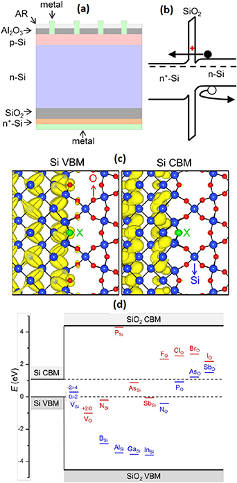
Figure 16. (a) and (b) One solution to decrease losses at the rear metal/n-Si contact by incorporating an ultrathin SiO2 tunneling layer for interface passivation. (c) Atomic model for the SiO2/Si interface that is free of the band-gap levels and shows a two times periodicity along the interface. Yellow isosurfaces present electron-level distributions for valence- and conduction-band levels. (d) Gap-levels induced by possible defects in SiO2. Blue lines show levels which tend to have negative charge while red lines have positive. Reproduced from Liu et al [274]. With the permission of AIP Publishing.
Download figure:
Standard image High-resolution imageAnother issue connecting the photonics device researcher and surface physicist arises from the question how the semiconductor n-type or p-type doping efficiency changes near the surface areas, and which methods are potential to increase the surface doping in order to decrease the contact resistivity [277–287]. A general rule is the higher doping the lower contact resistivity. However, the high surface doping also increases carrier recombination losses.
Donor activation energy (i.e. separation from the conduction band) has been found to increase at semiconductor surfaces [277, 278], but the reason(s) for this has remained unclear. Also it is still unclear how the embedded interface, for example, with an insulator film affects the doping activation barrier and thus the doping efficiency. Furthermore, unintentional interface impurities might change the doping atom bonding environment. The intentionally added hydrogen for the dangling bond passivation is expected to have a harmful effect on the doping efficiency [283].
To control the doping atom density at semiconductor surfaces, so-called monolayer doping has been developed [279–281]. To increase further the p-type doping at GaN, Lu et al [99] have deposited a Mg film on GaN and performed a proper post heating of Mg/GaN before the metal contact fabrication, while an oxidation of GaN surfaces has improved n-type doping [287].
Last but not least, the cleaning of a semiconductor surface is a very crucial step to decrease the contact resistivity. The high-quality starting template for a metal film enhances an epitaxial nature of the grown interface, which further decreases the density of point defects. For example, a coherent Ag/Si(111) interface has been recently found to decrease losses in the solar cell [288]. Furthermore, quantum mechanical simulations of atomic diffusion strengths [e.g. 179] at metal-semiconductor interface can clarify a tendency to the alloy formation. It can be expected that dry cleaning or etching methods, which are under an intense development [e.g. 289–291], become very useful to optimize also the contact interfaces in particular if these methods can be integrated with a metal-deposition instrument in situ manner without breaking a vacuum environment. It is worth noting that meaning of the dry cleaning methods is expected to increase in more general when three-dimensional structuring of device components increases; when trenches become deeper and more narrow, because the wet chemical methods do not perform properly for such structures.
4.6. Which might be potential approaches to develop atomic-scale protection of nanocrystals?
Nanocrystals can be readily linked to surface science because the surface areas of a nanocrystal are a significant portion of the whole material. Different semiconductor nanomaterials such as quantum dots (QDs) and nanowires have been investigated from the viewpoint of applications and fundamental properties [e.g. 36, 292–318]. Although STM and scanning tunneling spectroscopy (STS) are in general challenging for three-dimensionally structured nanomaterial surfaces, STM and STS have provided a unique local real-space probe for elucidating the atomic and electronic structures of individual nanocrystals [36, 295, 298, 302, 303, 305, 312]. Semiconductor nanocrystals are also potential materials for future photonic devices such as photodetectors, solar cells, and LEDs [292, 298, 299, 301, 304, 306–311, 313, 315, 317].
Indeed, InP QD containing LED devices have been recently commercialized [308, 317]. These non-toxic InP nanocrystals, called also colloidal QD, have been manufactured in chemical solutions. There are also other methods to prepare nanocrystals; for example, layer-by-layer deposition on solid templates (i.e. from bottom to top) or partial removing of the surrounding material via dry and/or wet etching methods (from top to down).
Irrespective of the nanocrystal fabrication method, the common issue is how to protect nanocrystals against environment-induced degradation of the material as a function of time. One solution has been to cover nanocrystals by a shell(s) which protects the core crystal. For instance, ZnS-capped InP and CdSe colloidal QDs are used in applications [e.g. 308, 310, 317]. However, elegant in-situ photoluminescence (PL) measurements of CdS + ZnS capped CdSe QDs during the exposure to different gases have revealed that shell-covered QDs are also sensitive to environment [310]. Higher PL intensity means lower density of defects. Interestingly water molecules adsorbed on QDs are beneficial to increase the PL intensity while a plasma exposure of QDs quickly decrease their PL intensity [310]. Furthermore, for passivating QDs by ALD, many metal precursors have been found harmful to QD luminescence [310] indicating that a care is needed to engineer the shell-covered nanocrystal surfaces for starting the deposition of the next capping film.
Recent study of InP colloidal QDs (figure 17) passivated with water-free benzoyl fluoride has shown that the used F-based treatment does not remove all oxidized phosphorus from the InP QD surface but still the luminescence properties of InP QDs improve [314]. The surface phosphorus with a low oxidation state has been found to be more harmful than the highly oxidized P to the luminescence [314], which is a promising result because it is not possible to avoid the incorporation of oxygen atoms into QD surfaces in applications. That finding is also consistent with the computational results for the InP interfaces [233].
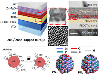
Figure 17. Top: scheme of colloidal quantum-dot (QD) LED containing ZnS/ZnSe-capped InP QD. Reproduced from Won et al [308]. With permission from Springer Nature. Bottom: hydrogen fluoride (HF) based treatment of InP QD, which improves luminescence intensity, causes formation of InF3 on QD and breakage of polychains of POx into separated POx molecules, marked by red circles in the atomic models Reproduced from Ubbink et al [314]. CC BY 4.0.
Download figure:
Standard image High-resolution imagePlasma is the common environment for semiconductor surfaces in device processes, for example, at the stages of etching of nanostructures (or mesas) and of film growth stages, but plasma interactions are also known to cause surface defects [319–327]. On the other hand, benefits of plasma sources include enhanced surface reactions at low semiconductor temperatures. The recent study (figure 18) has revealed effects of the plasma enhanced ALD growth of SiO2 in relation to an alternative method to grow SiO2 passivation layer for InGaN/GaN nano-LEDs using tetraethyl orthosilicate (TEOS) based sol–gel approach [315]. Before the SiO2 growth, dry-etching induced disorder or amorphization was removed from the nitride mesa sidewalls by wet chemistry. Recent results [325] show that a method combining ultraviolet light exposure and ozone for surface oxidation followed by HF-based wet etching removes effectively the dry etching defects.
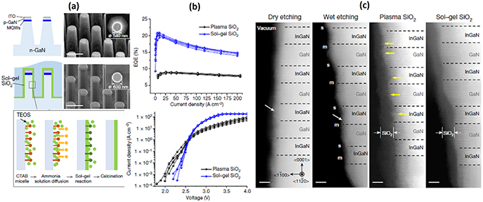
Figure 18. (a) Schematic structures and microscopy images for nano LED containing InGaN/GaN quantum wells. After dry etching of nanowire LED structures, their sidewalls were still etched wet chemically and passivated by TEOS-based spin-coated SiO2 film. (b) Passivation of sidewalls of nano LED was compared to plasma ALD-grown SiO2-coated nano LED. The new TEOS-based passivation increased the external quantum efficiency of nano LED and decreased the leakage current at the voltages lower than the diode threshold. (c) Transmission electron microscopy images of nano-LED sidewalls. After dry etching, the sidewall surface is amorphous. This disordered surface was removed by wet etching, which also increased a long-range roughness. Plasma ALD-grown SiO2 interface at sidewall included amorphous areas marked by yellow arrows. Reproduced from Sheen et al [315]. With permission from Springer Nature.
Download figure:
Standard image High-resolution imageFurthermore, the TEOS-based SiO2 passivation film decreased atomic interactions and amorphization at the mesa GaN interfaces, which increased the LED output efficiency and decreased the diode leakage current [315]. Future studies can clarify what kind of GaN surface termination provides a durable bonding to the adsorbed TEOS-based SiO2 nanocrystal material. Also, a well-justified atomic model for these GaN interfaces is helpful to understand atomic origins of the point defects that decrease radiative recombination and increase leakage current. The III–V nitride surfaces are an exception among semiconductors because the GaN-based surfaces remain largely crystalline although they often include significant amounts of oxygen and carbon. Furthermore, theoretical simulations for core-level binding-energy changes, based on the interface atomic models can confirm an intuitive identification of unusual Ga–Ga bonding structures [315].
Vertical sidewalls of three-dimensional nanostructures are of course much more challenging to measure by surface physics methods as compared to planar surfaces. One option to circumvent this problem is to prepare specific planar samples by using the same dry-etching and plasma parameters as for the device structuring [328]. Such planar 'model samples' can be expected to reflect the sidewall properties of devices, and can be measured efficiently by a large arsenal of standard surface-science tools. One potential direction to advance the device surface characterization is in-situ measurements [310, 329] in realistic chemical environments and pressures during the semiconductor surface reactions, instead of before and after the interface formation. Indeed catalysis community has taken such a step forward in metal surface studies to avoid so-called pressure gap [330–332].
4.7. Is it possible to avoid high-temperature degradation of SiC surface properties?
SiC is an emergent semiconductor in industry, which has been utilized particularly in devices where Si and III–V do not perform properly for commercial purposes. Such applications include electronic and photonic devices used in harsh conditions like at high temperatures or/and under intense radiation. High-power transistors and ultraviolet and particles detectors are examples of industrial SiC devices [e.g. 333–341]. 4H-SiC is the common crystal phase with a high indirect band gap of 3.3 eV which enables a low thermal-generation dark current even at elevated temperatures and a solar-blind UV detection (250–280 nm), as compared to the common Si detectors.
One specific challenge in manufacturing SiC devices is high temperature treatments up to 1700 °C which are mainly needed to activate the doping after implantation and to fabricate alloyed Ohmic contacts. However, the high temperatures cause the formation of crystal defects both in bulk and at surface regions. Thus, one relevant question is how SiC surfaces can be protected during the high temperature treatments. Second, an alternative doping method(s) might be considered to prepare p–n junctions via the re-growth of doped SiC layers at lowered temperatures. On the other hand, Schottky contact metal–semiconductor–metal structures provide an opportunity to develop SiC-based photodetectors via low temperature processing because the activation heating for doping implantation and alloyed Ohmic contacts are not necessarily needed. One benefit obtained from lowering the processing temperature is a decreased surface roughness which further has been found to decrease the dark leakage current of Schottky detectors [334].
Concerning the wet chemical cleaning of SiC, a very strong background knowledge obtained in the Si technology can be applied also in SiC processing. Furthermore, SiO2 is a natural oxide for SiC but the SiC oxidation has been found to cause higher interface defect density as compared SiO2/Si [236–238, 342]. However, including nitrogen at SiO2/SiC has been found to lead to a highly crystalline SiON/SiC interface (figure 19), which is also surprisingly stable in air [343–345]. This SiON/SiC with a (sqrt 3 × sqrt 3) structure is perhaps the only reconstruction so far which remains during prolonged air exposures. The high temperature exposure of SiC surfaces to H2 and following N2 gas flow at 1350 °C have been used to prepare this epitaxial SiON/SiC [343–345]. It is worth noting that no plasma source plasma source was used in preparing epitaxial SiON/SiC, consistent with the harmful plasma effects found for the crystallinity of GaN interfaces (figure 18). On the other hand, a plasma sources enables use of lower temperatures [346]. A thickness of the epitaxial SiON layer is 0.6 nm approximately, which provides a very potential tunneling barrier, for example, the photodetectors based on Schottky contacts (section 4.5). Future studies might clarify if it is possible to find low-temperature parameters to prepare crystalline SiON layers on SiC.
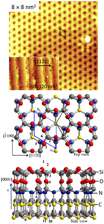
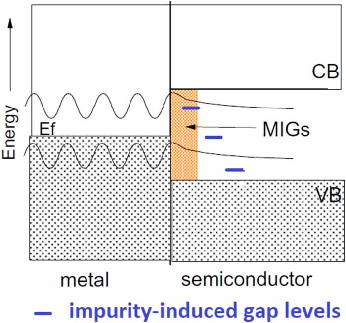
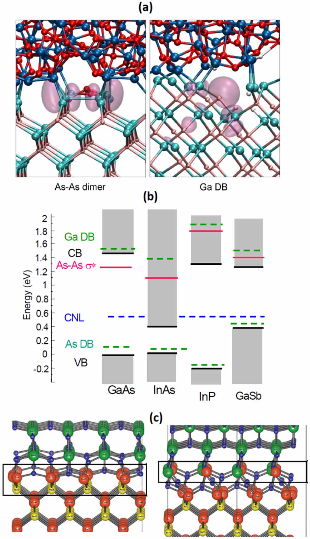
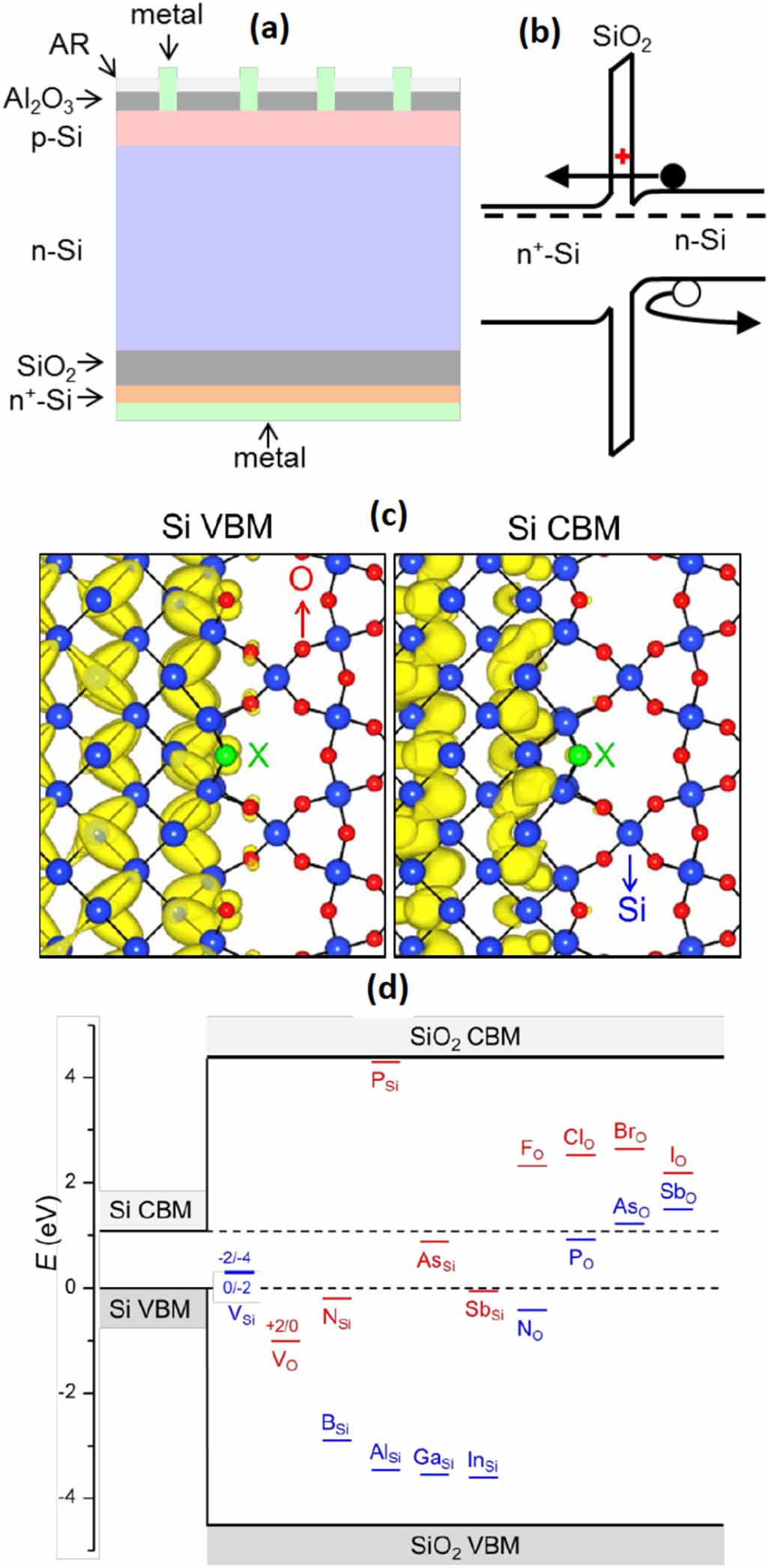
Figure 19. Top: crystalline and stable insulator layer of SiON (0.6 nm) formed at 6H- and 4H-SiC(0001) surfaces when SiC was heated first in H2 and then in N2 at 1350 °C. STM images show a stepped surface with a well-ordered (sqrt 3) × (sqrt 3) structure. Reprinted figure with permission from Shirasawa et al [344]. Copyright 2007 by the American Physical Society. Bottom: potential atomic model for a crystalline SiON/SiC(0001) interface. Reproduced from Shirasawa et al [345]. Copyright 2011, with permission from Elsevier.
Download figure:
Standard image High-resolution image
One relevant question to decrease the processing temperatures of SiC crystals concerns if it is possible to grow a highly doped layers at lowered temperatures with a reasonable crystalline quality and low defect density because the high temperature is particularly needed to activate the doping after implantation and to enable surface alloying SiC with metal(s) for Ohmic metal contacts. For such re-growth purposes of doped layers, the starting SiC surface properties have a significant effect. Concerning the SiC interface passivation, a specific feature of SiC devices is the required high-temperature operation up to 500 °C or even higher. This means that the SiC interface passivation needs to be unusually stable as well. Most likely, the hydrogen passivation used widely in the Si technology does not meet this high temperature stability.
4.8. Do two-dimensional semiconductors include surface defects?
In this article we have described the connecting subjects using examples of the traditional semiconductors. However, it is important to note there are several emergent material systems which are potential for future photonic devices. Indeed, it can be expected that use of novel materials increases in photonic industry as well, for example, via constructing hybrid materials with several critical interfaces. Two-dimensional (2D) semiconductors and perovskites are examples which have attracted great interest [e.g. 347–363]. Perovskite solar cells have been recently commercialized [347].
Some of the above-described issues such as the development of surface passivation and Ohmic contacts are relevant to the research of emergent materials too. Each system has still own specific challenges, which on the other hand provide new connection opportunities. Surface areas form a significant part of the whole 2D semiconductor materials. However, their surfaces should be relatively inert without the dangling bonds, as compared to many traditional semiconductors with the covalent bonding structure. We are not able to review all those groundbreaking studies of 2D semiconductors, not to mention for other emergent photonic materials. In contrast, we point out here couple interesting properties in relation to the items introduced in section 4.
STM has been an essential tool to reveal a real structure and quality of practical 2D surfaces [348, 350, 354, 358]. Naturally, every material includes defects, and STM has been helpful to understand local defect formation at 2D surfaces also. Furthermore, the surface defects affect oxidation and metal contact formation on 2D semiconductors. Although the inherent inertness of 2D surfaces can be expected to decrease a rate of surface oxidation, it has been presented that it is not possible to avoid incorporation of oxygen atoms even into 2D surfaces, and how difficult it is to detect oxygen atoms [358]. On the other hand, it has been found that a proper oxygen incorporation does not cause the defect levels in the band gap [352, 358, 363], which supports a benefit of controlling the oxidation. Indeed, if we think the success of Si technology, one key factor has been a careful control of the Si surface oxidation. The second key factor has been controlling the electron and hole doping of semiconductors. Toward that, careful modification of the surface chemistry and doping is highly relevant [e.g. 359, 362, 364–366] because the traditional methods for bulk-like doping of 3D crystals cannot be efficiently employed. We assume that the whole semiconductor field gets a benefit from the development of novel surface passivation, doping, and contact methods for 2D materials.
5. Summary
We hope that the presented article is useful to both communities: photonics and surface science, encouraging two communities to increase bilateral collaboration. Photonic device researchers and surface physicists have typically approached the semiconductor surface properties from different perspectives with different methods. Our aim has been to discuss some semiconductor surface-related issues which might provide extra synergy between the two disciplines. The common goal for the reviewed subjects is to decrease the semiconductor surface-related optoelectronic losses in photonic devices by adding understanding of semiconductor interfaces.
Wet chemical treatment(s) is the basic procedure in manufacturing any semiconductor device. The literature review indicates that Si(111) might be an exception among semiconductor surfaces because a proper wet chemical treatment provides almost an ideal, atomically smooth and well crystalline H-terminated Si(111)(1 × 1)-H surface, as evidenced by STM. However, a cleaned semiconductor surface is not necessarily crystalline in general. Future studies will clarify whether the high-quality starting surface, similar to Si(111)(1 × 1)-H, is obtained by wet chemical methods for other semiconductors and crystalline planes, of which understanding is relevant to the development of three-dimensional device structures such as mesa sidewalls, nanowires and laser diode mirrors.
The smoothness and ordering of a starting semiconductor surface affects sharpness and crystallinity of an interface grown on the semiconductor. In addition to the wet chemistry, dry cleaning methods and their effects on surface structures provide a complementary connecting subject. STM has been found to be a very useful characterization method to understand which treatments are most potential to improve the atomic level smoothness and order on semiconductor surfaces.
It is not possible to avoid the incorporation of oxygen atoms at semiconductor interfaces of devices. Thus, it is relevant to develop the methods for controlling the oxygen incorporation and the properties of semiconductor surface oxides. The surface oxidation typically increases the disorder in the atomic structure, which further increases the point defect density. The computational physics methods have provided irreplaceable atomic-scale information about defect-level formation and electronic band structures of oxidized semiconductor surfaces. Various theoretical models, which provide the semiconductor band gap free of defect levels, have been constructed for oxide/semiconductor systems giving a guideline to prepare the interfaces for low-loss devices in practice. Still preparing an insulator/semiconductor interface with the gap level density lower than 1‧1010 cm−2eV−1 is a great challenge for many devices. Toward that target, it is probably crucial to find for each semiconductor a proper combination of different techniques available in a large arsenal of the semiconductor passivation methods.
Metal/semiconductor interfaces are even more challenging concerning the carriers' surface recombination because of the presence of MIGS, in addition to the point-defect induced gap levels. Because many photonic devices do not require ultra-low contact resistivity for their high performance, the ultrathin insulator tunneling barriers are under development to reduce the effect of MIGS. Creating proper gap levels in the area of a tunneling barrier is expected to enhance the carriers' transmission through such a passivated and selective contact.
SiC is an emergent device material of which interfaces are a challenge. It is expected that low temperature methods to increase the surface doping and to prepare the Ohmic contacts will reduce the high-temperature induced surface degradation and energy consumption in SiC device manufacturing. The device durability criteria in harsh operation conditions set also unusual requirements for the passivation of SiC device interfaces.
Acknowledgments
This work has been supported by the following Research Council of Finland projects: COLO #338973, COLO #338974, HyperGer #354199, and NIR #331313 and via to the Flagship on Photonics Research and Innovation 'PREIN' funded by Academy of Finland. This work has been supported also by the following Business Finland projects: FemtoBlack #7479/31/2019 and SISUPROCO #1671/31/2018.
Data availability statement
All data that support the findings of this study are included within the article.
Appendix:
Table 1 shows selected surface recombination velocities measured for Si, Ge, IIII–V, and SiC interfaces with some other properties, in chronological order. Footnotes:  and
and  are determined at injection level of a
7 × 1014 cm−3, b
1 × 1015 cm−3, c
1 × 1014 cm−3, d
2 × 1014 cm−3 and e
5 × 1015 cm−3. Values in parenthesis are calculated from reported values.
are determined at injection level of a
7 × 1014 cm−3, b
1 × 1015 cm−3, c
1 × 1014 cm−3, d
2 × 1014 cm−3 and e
5 × 1015 cm−3. Values in parenthesis are calculated from reported values.
Table 1. Comparison of surface recombination velocities for selected semiconductors, which vary depending on a surface structure and its passivation.
| Passivation layer | Substrate |
 (μs) (μs) |
 (cm s−1) (cm s−1) |
 (cm−2 eV−1) (cm−2 eV−1) |
 (cm−2) (cm−2) | References | ||
|---|---|---|---|---|---|---|---|---|
| Type Si | Thickness (μm) | Resistivity (Ω cm) | ||||||
| Measured during HF-based immersion | n-Si | 250 | 150 | 0.25 | (2.5 × 10⁷) | No significant band bending | [161] | |
| SiO2 | p-Si | Boron doping by diffusion 3 × 1019 cm−3 | 1640 | [367] | ||||
| Metal film of Al | p-Si | Boron diffused surface 3 × 1019 cm−3 | 1 × 10⁵ | [367] | ||||
| PECVD SiN | p-Si | 1 | 4 | [368] | ||||
| SiNx b | n-Si | 275 | 90 | 10 000 | 1.38 | [369] | ||
| Al2O3 by plasma ALD + post heating in N2 at 425 °C | n-Si | 275 | 2 | 7000 | 2 | ∼1013 | [370] | |
| Al2O3 b | Textured p-Si | 525 | 17–24 | ∼10 000 | 22 | [371] | ||
| Al2O3 b | Textured n-Si | 445 | 3.37 ± 0.5 | 3000 | 7 | −9.9 × 10¹² | [372] | |
| SiO2 b | n-Si | 195 | 1 | 5643 | 0.4 | 3 × 10¹¹ | 1.7 × 10¹² | [261] |
| ZnO:Be | n-Si | 280 | 3 | 1530 | 4.8 | [373] | ||
| TOPCon (a-SiCx )c | n-Si | 480 | 1000 | 500 000 | (0.048) | [374] | ||
| Al2O3/SiO2 multilayersb | n-Si | 200 | 10 | 19 000 | (0.53) | −1 × 10¹³ | [375] | |
| Hot-water induced SiO2 | Sidewalls of Si(110) | 50 | [376] | |||||
| Ge | ||||||||
| Wet oxidation | n-Ge | 300 | 10 | 80 | [377] | |||
| Dry oxidation | p-Ge | 300 | 10 | 80 | [377] | |||
| Amorphous silicon | p-Ge | 170 | 10 | 530 | 17 | [378] | ||
| Amorphous Si:H/Al2O3 b | n-Ge | 325 ± 25 | 1–3 | 7 | −9 × 10¹² | [379] | ||
| Al2O3 a | n-Ge | 175 | 18–25 | 1400 | 7 | −2.3 × 10¹² | [380] | |
| a-SiCx /Al2O3 b | p-Ge | 175 | 1.2 | 18 | −3.2 × 10¹² | [381] | ||
| SiNx c | n-Ge | 175 | 5–15 | 150 | 58 | 1 × 10¹² | [382] | |
| SiNx /Al2O3 c | n-Ge | 175 | 5–15 | 500 | 17 | 4 × 10¹¹ | −1.6 × 10¹¹ | [382] |
| SiO2/Al2O3 c | n-Ge | 189 | 17–39 | 1.3 | 5 × 10¹¹ | 8.5 × 10¹¹ | [383] | |
| Al2O3 d | Textured n-Ge | 187 | 18–25 | ∼30 | [384] | |||
| III–V | ||||||||
| Ga2O3 | n- or p-GaAs | 4000 | [385] | |||||
| Without passivation | Bare n-GaAs or p-GaAs | 1 × 10⁷ | [385] | |||||
| Wet chemical (NH4)2S | InAs/GaSb stack | 1000 | [386] | |||||
| Without passivation | InP nanowires | 170 | [387] | |||||
| (NH4)2S + SiO2 | InGaAsP | 4000 | [388] | |||||
| Al2O3 | InAsSb nanowires | 1000 | [389] | |||||
| SiC | ||||||||
| Chemical mechanical polished wafer | Silicon terminated 4H-SiC | 1.4 | 2000 | [390] | ||||
| Chemical mechanical polished wafer | Carbon-terminated 4H-SiC | 1.2 | 5500 | [390] | ||||
| Mesa sidewall | 4H-SiC | 6 × 10⁵ | [391] | |||||
| Oxidized surface at 1400 °C | Epitaxial 4H-SiC | 250 | n-type doping 5 × 1013 cm- | 600 | [392] | |||
Note: The inherent bulk carrier lifetime (equation 1) is smaller for direct band-gap III-V crystals than for indirect band-gap semiconductors due to a high radiative recombination rate in III-V crystals.