当前位置:
X-MOL 学术
›
Prog. Photovoltaics
›
论文详情
Our official English website, www.x-mol.net, welcomes your feedback! (Note: you will need to create a separate account there.)
Axial p‐n junction design and characterization for InP nanowire array solar cells
Progress in Photovoltaics ( IF 6.7 ) Pub Date : 2018-11-05 , DOI: 10.1002/pip.3083 Qian Gao 1 , Ziyuan Li 1 , Li Li 2 , Kaushal Vora 2 , Zhe Li 3 , Ahmed Alabadla 1 , Fan Wang 1 , Yanan Guo 1 , Kun Peng 1 , Yesaya C. Wenas 1 , Sudha Mokkapati 1 , Fouad Karouta 2 , Hark Hoe Tan 1 , Chennupati Jagadish 1 , Lan Fu 1
Progress in Photovoltaics ( IF 6.7 ) Pub Date : 2018-11-05 , DOI: 10.1002/pip.3083 Qian Gao 1 , Ziyuan Li 1 , Li Li 2 , Kaushal Vora 2 , Zhe Li 3 , Ahmed Alabadla 1 , Fan Wang 1 , Yanan Guo 1 , Kun Peng 1 , Yesaya C. Wenas 1 , Sudha Mokkapati 1 , Fouad Karouta 2 , Hark Hoe Tan 1 , Chennupati Jagadish 1 , Lan Fu 1
Affiliation
|
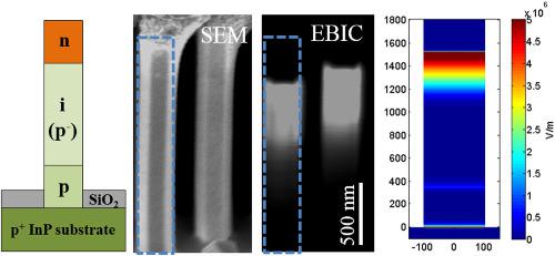
In this work, InP nanowire (NW) array solar cells with different axial p‐i‐n junction designs were investigated. The optical properties of the different NW structures were characterized through a series of microphotoluminescence measurements to extract important material parameters such as minority carrier lifetimes and internal quantum efficiencies. A glancing angle sputtering deposition technique has been developed to enable a direct visualization of the p‐n junctions in the vertical array of InP NW solar cells (NWSCs) using electron beam‐induced current (EBIC) technique. Based on EBIC and electrical simulation, it is found that the background doping in NWSC significantly affects the junction position. By modifying the junction design, the width and position of the p‐n junction can be varied effectively. By employing a p‐p−‐n structure, a high junction position (>1 μm from the substrate) and wide depletion width have been achieved as confirmed by EBIC measurement. Moreover, the NW growth substrate does not show any influence on the device behavior due to the fully decoupled junction position, indicating a promising structural design for future development of high‐performance, low‐cost flexible NW devices.
中文翻译:

InP纳米线阵列太阳能电池的轴向p‐n结设计与表征
在这项工作中,研究了具有不同轴向p-i-n结设计的InP纳米线(NW)阵列太阳能电池。通过一系列微光致发光测量来表征不同NW结构的光学性质,以提取重要的材料参数,例如少数载流子寿命和内部量子效率。已经开发出掠射角溅射沉积技术,以使用电子束感应电流(EBIC)技术直接观察InP NW太阳能电池(NWSCs)垂直阵列中的p-n结。基于EBIC和电学模拟,发现NWSC中的背景掺杂显着影响结位置。通过修改结设计,可以有效地改变PN结的宽度和位置。通过使用ap-p− ‐n结构,通过EBIC测量证实,实现了较高的结位置(距衬底1μm)和较宽的耗尽层宽度。此外,由于结位置完全解耦,NW生长衬底对器件的性能没有任何影响,这表明对高性能,低成本柔性NW器件的未来发展而言,其结构设计很有希望。
更新日期:2018-11-05
中文翻译:
InP纳米线阵列太阳能电池的轴向p‐n结设计与表征
在这项工作中,研究了具有不同轴向p-i-n结设计的InP纳米线(NW)阵列太阳能电池。通过一系列微光致发光测量来表征不同NW结构的光学性质,以提取重要的材料参数,例如少数载流子寿命和内部量子效率。已经开发出掠射角溅射沉积技术,以使用电子束感应电流(EBIC)技术直接观察InP NW太阳能电池(NWSCs)垂直阵列中的p-n结。基于EBIC和电学模拟,发现NWSC中的背景掺杂显着影响结位置。通过修改结设计,可以有效地改变PN结的宽度和位置。通过使用ap-p− ‐n结构,通过EBIC测量证实,实现了较高的结位置(距衬底1μm)和较宽的耗尽层宽度。此外,由于结位置完全解耦,NW生长衬底对器件的性能没有任何影响,这表明对高性能,低成本柔性NW器件的未来发展而言,其结构设计很有希望。


 京公网安备 11010802027423号