npj 2D Materials and Applications ( IF 9.7 ) Pub Date : 2018-11-05 , DOI: 10.1038/s41699-018-0082-2 June Yeong Lim , Minju Kim , Yeonsu Jeong , Kyeong Rok Ko , Sanghyuck Yu , Hyung Gon Shin , Jae Young Moon , Young Jai Choi , Yeonjin Yi , Taekyeong Kim , Seongil Im
|
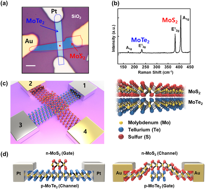
Two-dimensional (2D) transition metal dichalcogenides (TMDs)-based van der Waals (vdW) PN junctions have been used for heterojunction diodes, which basically utilize out-of-plane current across the junction interface. In fact, the same vdW PN junction structure can be utilized for another important device application, junction field effect transistors (JFETs), where in-plane current is possible along with 2D–2D heterojunction interface. Moreover, the 2D TMD-based JFET can use both p- and n-channel for low voltage operation, which might be its unique feature. Here we report vdW JFETs as an in-plane current device with heterojunction between semiconducting p- and n-TMDs. Since this vdW JFET would have low-density traps at the vdW interface unlike 2D TMD-based metal insulator semiconductor field effect transistors (MISFETs), little hysteresis of 0.0–0.1 V and best subthreshold swing of ~100 mV/dec were achieved. Easy saturation was observed either from n-channel or p-channel JFET as another advantage over 2D MISFETs, exhibiting early pinch-off at ~1 V. Operational gate voltage for threshold was near 0 V and our highest mobility reaches to ~>500 cm2/V·s for n-channel JFET with MoS2 channel. For 1 V JFET operation, our best ON/OFF current ratio was observed to be ~104.
中文翻译:
带有n沟道和p沟道过渡金属二卤化物的Van der Waals结型场效应晶体管
基于二维(2D)过渡金属二硫化碳(TMDs)的范德华(vdW)PN结已用于异质结二极管,其基本上利用了跨结界面的平面外电流。实际上,相同的vdW PN结结构可用于另一个重要的器件应用,即结场效应晶体管(JFET),其中平面电流与2D–2D异质结接口一起可能出现。此外,基于2D TMD的JFET可以同时使用p通道和n通道进行低压操作,这可能是其独特的功能。在这里,我们将vdW JFET报告为面内电流器件,在半导体p-TMD和n-TMD之间具有异质结。由于此vdW JFET在vdW接口处将具有低密度陷阱,这与基于2D TMD的金属绝缘体半导体场效应晶体管(MISFET)不同,因此几乎没有滞后0。获得了0-0.1 V的最佳亚阈值摆幅,约为100 mV / dec。与2D MISFET相比,n沟道或p沟道JFET易于观察到饱和,这是其另一个优势,在〜1 V时表现出早期夹断。阈值的工作栅极电压接近0 V,我们的最高迁移率达到〜> 500 cm对于具有MoS 2通道的n通道JFET,为2 / V·s 。对于1 V JFET操作,我们观察到的最佳开/关电流比为〜10 4 。


 京公网安备 11010802027423号