npj 2D Materials and Applications ( IF 9.7 ) Pub Date : 2018-11-02 , DOI: 10.1038/s41699-018-0080-4 Tiantian Li , Dun Mao , Nick W. Petrone , Robert Grassi , Hao Hu , Yunhong Ding , Zhihong Huang , Guo-Qiang Lo , James C. Hone , Tony Low , Chee Wei Wong , Tingyi Gu
|
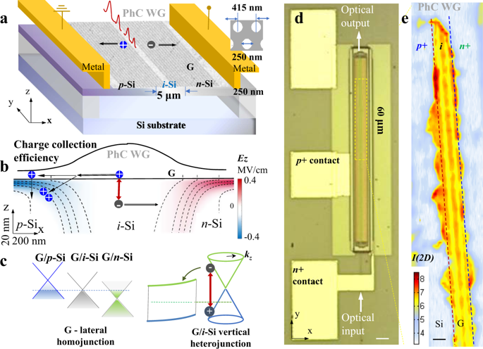
Sufficiently large depletion region for photocarrier generation and separation is a key factor for two-dimensional material optoelectronic devices, but only a few device configurations have been explored for a deterministic control over the space charge region area in graphene with convincing scalability. Here we investigate a graphene-silicon p-i-n photodiode defined in a foundry processed planar photonic crystal waveguide structure, achieving visible—near-infrared, zero-bias, and ultrafast photodetection. Graphene is electrically contacting to the wide intrinsic region of silicon and extended to the p an n doped region, functioning as the primary photocarrier conducting channel for electronic gain. Graphene significantly improves the device speed through ultrafast out-of-plane interfacial carrier transfer and the following in-plane built-in electric field assisted carrier collection. More than 50 dB converted signal-to-noise ratio at 40 GHz has been demonstrated under zero bias voltage, the quantum efficiency could be further amplified by hot carrier gain on graphene-i Si interface and avalanche process on graphene-doped Si interface. With the device architecture fully defined by nanomanufactured substrate, this work demonstrates post-fabrication-free two-dimensional material active silicon photonic devices.
中文翻译:
混合硅光电二极管在石墨烯引脚结中的空间控制静电掺杂
足够大的耗尽区用于光生载流子和分离是二维材料光电器件的关键因素,但只有极少数器件配置可用于确定性地控制石墨烯中的空间电荷区,并具有令人信服的可扩展性。在这里,我们研究了在铸造加工的平面光子晶体波导结构中定义的石墨烯-硅针型光电二极管,实现了可见光,近红外光,零偏压和超快光电检测。石墨烯是电接触硅的宽征区并延伸至p的Ñ掺杂区,用作电子增益的主要光载流子传导通道。石墨烯通过超快的面外界面载流子传输和随后的面内内置电场辅助载流子收集,大大提高了设备速度。在零偏置电压下,已证明在40 GHz频率下具有超过50 dB的转换信噪比,量子效率可以通过石墨烯-i Si界面上的热载流子增益和石墨烯掺杂的Si界面上的雪崩过程来进一步放大。借助纳米制造基板完全定义的器件架构,这项工作演示了免制造后的二维材料有源硅光子器件。


 京公网安备 11010802027423号