Chemical Physics Letters ( IF 2.8 ) Pub Date : 2018-10-29 , DOI: 10.1016/j.cplett.2018.10.068 Arash Boochani , Elmira Sartipi , Shahram Solaymani
|
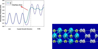
Half-metallic, optical and band offsets properties of CrSb/KCl [001] interface have been calculated within the density functional theory (DFT) framework using FP-LAPW+lo method. We found that the CrSb/KCl [001] heterojunction retain perfect half-metallic character with 0.95eV and 1.5eV spin flip gap at spin down, using GGA and mbj approximations, resprctively. The 0.03meV electrostatic potential gap between CrSb film and KCl substrate demonstrate that the CrSb film is the good spin electron source for injection to the KCl film. The optical coefficients such as real and imaginary parts of dielectric function, reflection, refraction, extinction and energy loss function indices have been shown the good optical response in the visible area. The band offset parameters of CrSb/KCl [001] interface are of the type-I model with great amount of ФB and χ potentials.
中文翻译:
CrSb / KCl [001]界面中的带偏移,半金属和光学行为:通过DFT计算
在FP-LAPW + lo方法的密度泛函理论(DFT)框架内,已计算出CrSb / KCl [001]界面的半金属,光学和带偏移特性。我们发现,CrSb / KCl [001]异质结保留了完美的半金属特性,分别使用GGA和mbj近似在向下旋转时具有0.95eV和1.5eV的旋转翻转间隙。CrSb薄膜与KCl衬底之间的0.03meV静电势隙表明,CrSb薄膜是注入KCl薄膜的良好自旋电子源。光学系数,例如介电函数的实部和虚部,反射,折射,消光和能量损失函数指数,已经显示出在可见光区域的良好光学响应。CrSb / KCl [001]接口的带偏移参数属于I型模型,具有很大的ФB和χ势。


 京公网安备 11010802027423号