Our official English website, www.x-mol.net, welcomes your feedback! (Note: you will need to create a separate account there.)
High‐Performance Wafer‐Scale MoS2 Transistors toward Practical Application
Small ( IF 13.3 ) Pub Date : 2018-10-16 , DOI: 10.1002/smll.201803465 Hu Xu 1 , Haima Zhang 1 , Zhongxun Guo 1 , Yuwei Shan 2 , Shiwei Wu 2 , Jianlu Wang 3 , Weida Hu 3 , Hanqi Liu 4 , Zhengzong Sun 4 , Chen Luo 5 , Xing Wu 5 , Zihan Xu 6 , David Wei Zhang 1 , Wenzhong Bao 1 , Peng Zhou 1
Small ( IF 13.3 ) Pub Date : 2018-10-16 , DOI: 10.1002/smll.201803465 Hu Xu 1 , Haima Zhang 1 , Zhongxun Guo 1 , Yuwei Shan 2 , Shiwei Wu 2 , Jianlu Wang 3 , Weida Hu 3 , Hanqi Liu 4 , Zhengzong Sun 4 , Chen Luo 5 , Xing Wu 5 , Zihan Xu 6 , David Wei Zhang 1 , Wenzhong Bao 1 , Peng Zhou 1
Affiliation
|
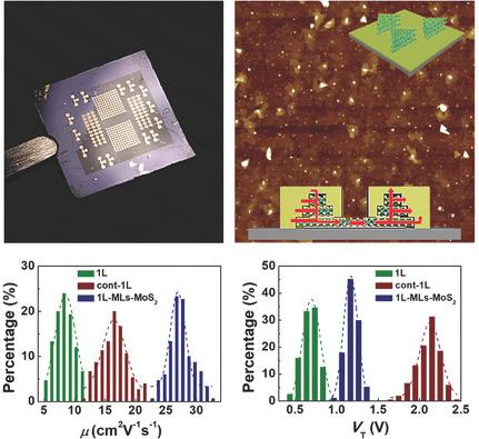
Atomic thin transition‐metal dichalcogenides (TMDs) are considered as an emerging platform to build next‐generation semiconductor devices. However, to date most devices are still based on exfoliated TMD sheets on a micrometer scale. Here, a novel chemical vapor deposition synthesis strategy by introducing multilayer (ML) MoS2 islands to improve device performance is proposed. A four‐probe method is applied to confirm that the contact resistance decreases by one order of magnitude, which can be attributed to a conformal contact by the extra amount of exposed edges from the ML‐MoS2 islands. Based on such continuous MoS2 films synthesized on a 2 in. insulating substrate, a top‐gated field effect transistor (FET) array is fabricated to explore key metrics such as threshold voltage (V
T) and field effect mobility (μFE) for hundreds of MoS2 FETs. The statistical results exhibit a surprisingly low variability of these parameters. An average effective μFE of 70 cm2 V−1 s−1 and subthreshold swing of about 150 mV dec−1 are extracted from these MoS2 FETs, which are comparable to the best top‐gated MoS2 FETs achieved by mechanical exfoliation. The result is a key step toward scaling 2D‐TMDs into functional systems and paves the way for the future development of 2D‐TMDs integrated circuits.
中文翻译:

高性能晶圆级MoS2晶体管在实际应用中的应用
原子薄的过渡金属二硫化碳(TMD)被认为是构建下一代半导体器件的新兴平台。然而,迄今为止,大多数设备仍基于微米级的剥落的TMD薄板。在此,提出了一种通过引入多层(ML)MoS 2岛来改善器件性能的新型化学气相沉积合成策略。应用四探针方法来确认接触电阻降低一个数量级,这可以归因于ML-MoS 2岛中多余边缘的额外接触,从而形成了共形接触。基于这种连续的MoS 2在2英寸绝缘基板上合成薄膜后,制造了一个顶部栅极场效应晶体管(FET)阵列,以探索关键指标,例如数百个MoS 2 FET的阈值电压(V T)和场效应迁移率(μFE)。统计结果显示出这些参数的出乎意料的低可变性。从这些MoS 2 FET中提取了70 cm 2 V -1 s -1的平均有效μFE和约150 mV dec -1的亚阈值摆幅,与最佳的门控MoS 2相当通过机械剥离实现的FET。结果是朝着将2D-TMD扩展到功能系统的关键一步,为2D-TMD集成电路的未来发展铺平了道路。
更新日期:2018-10-16
中文翻译:
高性能晶圆级MoS2晶体管在实际应用中的应用
原子薄的过渡金属二硫化碳(TMD)被认为是构建下一代半导体器件的新兴平台。然而,迄今为止,大多数设备仍基于微米级的剥落的TMD薄板。在此,提出了一种通过引入多层(ML)MoS 2岛来改善器件性能的新型化学气相沉积合成策略。应用四探针方法来确认接触电阻降低一个数量级,这可以归因于ML-MoS 2岛中多余边缘的额外接触,从而形成了共形接触。基于这种连续的MoS 2在2英寸绝缘基板上合成薄膜后,制造了一个顶部栅极场效应晶体管(FET)阵列,以探索关键指标,例如数百个MoS 2 FET的阈值电压(V T)和场效应迁移率(μFE)。统计结果显示出这些参数的出乎意料的低可变性。从这些MoS 2 FET中提取了70 cm 2 V -1 s -1的平均有效μFE和约150 mV dec -1的亚阈值摆幅,与最佳的门控MoS 2相当通过机械剥离实现的FET。结果是朝着将2D-TMD扩展到功能系统的关键一步,为2D-TMD集成电路的未来发展铺平了道路。


 京公网安备 11010802027423号