Our official English website, www.x-mol.net, welcomes your feedback! (Note: you will need to create a separate account there.)
Solution-processable 2D semiconductors for high-performance large-area electronics
Nature ( IF 64.8 ) Pub Date : 2018-10-01 , DOI: 10.1038/s41586-018-0574-4 Zhaoyang Lin , Yuan Liu , Udayabagya Halim , Mengning Ding , Yuanyue Liu , Yiliu Wang , Chuancheng Jia , Peng Chen , Xidong Duan , Chen Wang , Frank Song , Mufan Li , Chengzhang Wan , Yu Huang , Xiangfeng Duan
Nature ( IF 64.8 ) Pub Date : 2018-10-01 , DOI: 10.1038/s41586-018-0574-4 Zhaoyang Lin , Yuan Liu , Udayabagya Halim , Mengning Ding , Yuanyue Liu , Yiliu Wang , Chuancheng Jia , Peng Chen , Xidong Duan , Chen Wang , Frank Song , Mufan Li , Chengzhang Wan , Yu Huang , Xiangfeng Duan
|
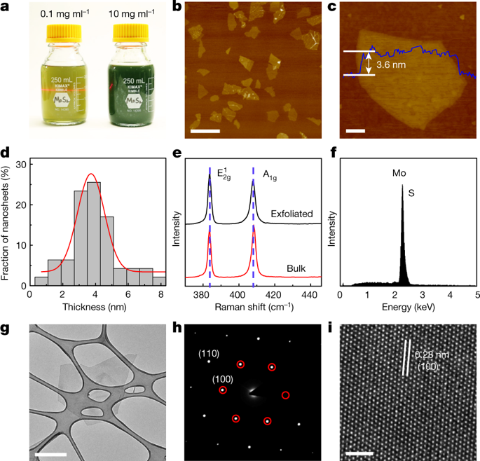
Two-dimensional (2D) materials, consisting of atomically thin crystal layers bound by the van der Waals force, have attracted much interest because of their potential in diverse technologies, including electronics, optoelectronics and catalysis1–10. In particular, solution-processable 2D semiconductor (such as MoS2) nanosheets are attractive building blocks for large-area thin-film electronics. In contrast to conventional zero- and one-dimensional nanostructures (quantum dots and nanowires, respectively), which are typically plagued by surface dangling bonds and associated trapping states, 2D nanosheets have dangling-bond-free surfaces. Thin films created by stacking multiple nanosheets have atomically clean van der Waals interfaces and thus promise excellent charge transport11–15. However, preparing high-quality solution-processable 2D semiconductor nanosheets remains a challenge. For example, MoS2 nanosheets and thin films produced using lithium intercalation and exfoliation are plagued by the presence of the metallic 1T phase and poor electrical performance (mobilities of about 0.3 square centimetres per volt per second and on/off ratios of less than 10)2,12, and materials produced by liquid exfoliation exhibit an intrinsically broad thickness distribution, which leads to poor film quality and unsatisfactory thin-film electrical performance (mobilities of about 0.4 square centimetres per volt per second and on/off ratios of about 100)14,16,17. Here we report a general approach to preparing highly uniform, solution-processable, phase-pure semiconducting nanosheets, which involves the electrochemical intercalation of quaternary ammonium molecules (such as tetraheptylammonium bromide) into 2D crystals, followed by a mild sonication and exfoliation process. By precisely controlling the intercalation chemistry, we obtained phase-pure, semiconducting 2H-MoS2 nanosheets with a narrow thickness distribution. These nanosheets were then further processed into high-performance thin-film transistors, with room-temperature mobilities of about 10 square centimetres per volt per second and on/off ratios of 106 that greatly exceed those obtained for previous solution-processed MoS2 thin-film transistors. The scalable fabrication of large-area arrays of thin-film transistors enabled the construction of functional logic gates and computational circuits, including an inverter, NAND, NOR, AND and XOR gates, and a logic half-adder. We also applied our approach to other 2D materials, including WSe2, Bi2Se3, NbSe2, In2Se3, Sb2Te3 and black phosphorus, demonstrating its potential for generating versatile solution-processable 2D materials.By intercalating large ammonium molecules to exfoliate MoS2 with preservation of the 2H-phase, highly uniform solutionprocessable 2D semiconductor nanosheets are obtained for the scalable fabrication of large-area thin-film electronics.
中文翻译:

用于高性能大面积电子设备的可解决方案处理的 2D 半导体
二维 (2D) 材料由范德华力束缚的原子级薄晶体层组成,因其在电子学、光电子学和催化等多种技术中的潜力而引起了广泛关注1-10。特别是,可溶液加工的 2D 半导体(如 MoS2)纳米片是大面积薄膜电子器件的有吸引力的构建块。与传统的零维和一维纳米结构(分别为量子点和纳米线)相比,它们通常受到表面悬挂键和相关捕获状态的困扰,而二维纳米片具有无悬挂键的表面。通过堆叠多个纳米片形成的薄膜具有原子级清洁的范德华界面,因此有望实现出色的电荷传输 11-15。然而,制备高质量的溶液可加工二维半导体纳米片仍然是一个挑战。例如,使用锂嵌入和剥离生产的 MoS2 纳米片和薄膜受到金属 1T 相的存在和较差的电气性能(迁移率约为 0.3 平方厘米/伏/秒和开/关比小于 10)的困扰2 ,12,并且通过液体剥离生产的材料表现出本质上较宽的厚度分布,这导致薄膜质量差和薄膜电性能不令人满意(迁移率约为 0.4 平方厘米/伏/秒,开/关比约为 100)14 ,16,17。在这里,我们报告了一种制备高度均匀、可溶液加工、相纯半导体纳米片的通用方法,这涉及将季铵分子(如四庚基溴化铵)电化学嵌入二维晶体,然后进行温和的超声处理和剥离过程。通过精确控制插层化学,我们获得了相纯、具有窄厚度分布的半导体 2H-MoS2 纳米片。然后将这些纳米片进一步加工成高性能薄膜晶体管,室温迁移率约为每秒每伏 10 平方厘米,开/关比为 106,大大超过先前溶液处理的 MoS2 薄膜晶体管。大面积薄膜晶体管阵列的可扩展制造使功能逻辑门和计算电路的构建成为可能,包括反相器、NAND、NOR、AND 和 XOR 门,和一个逻辑半加器。我们还将我们的方法应用于其他 2D 材料,包括 WSe2、Bi2Se3、NbSe2、In2Se3、Sb2Te3 和黑磷,展示了其生成通用溶液可加工 2D 材料的潜力。通过插入大铵分子来剥离 MoS2,同时保留 2H-阶段,获得了高度均匀的可溶液加工的 2D 半导体纳米片,用于大面积薄膜电子的可扩展制造。
更新日期:2018-10-01
中文翻译:
用于高性能大面积电子设备的可解决方案处理的 2D 半导体
二维 (2D) 材料由范德华力束缚的原子级薄晶体层组成,因其在电子学、光电子学和催化等多种技术中的潜力而引起了广泛关注1-10。特别是,可溶液加工的 2D 半导体(如 MoS2)纳米片是大面积薄膜电子器件的有吸引力的构建块。与传统的零维和一维纳米结构(分别为量子点和纳米线)相比,它们通常受到表面悬挂键和相关捕获状态的困扰,而二维纳米片具有无悬挂键的表面。通过堆叠多个纳米片形成的薄膜具有原子级清洁的范德华界面,因此有望实现出色的电荷传输 11-15。然而,制备高质量的溶液可加工二维半导体纳米片仍然是一个挑战。例如,使用锂嵌入和剥离生产的 MoS2 纳米片和薄膜受到金属 1T 相的存在和较差的电气性能(迁移率约为 0.3 平方厘米/伏/秒和开/关比小于 10)的困扰2 ,12,并且通过液体剥离生产的材料表现出本质上较宽的厚度分布,这导致薄膜质量差和薄膜电性能不令人满意(迁移率约为 0.4 平方厘米/伏/秒,开/关比约为 100)14 ,16,17。在这里,我们报告了一种制备高度均匀、可溶液加工、相纯半导体纳米片的通用方法,这涉及将季铵分子(如四庚基溴化铵)电化学嵌入二维晶体,然后进行温和的超声处理和剥离过程。通过精确控制插层化学,我们获得了相纯、具有窄厚度分布的半导体 2H-MoS2 纳米片。然后将这些纳米片进一步加工成高性能薄膜晶体管,室温迁移率约为每秒每伏 10 平方厘米,开/关比为 106,大大超过先前溶液处理的 MoS2 薄膜晶体管。大面积薄膜晶体管阵列的可扩展制造使功能逻辑门和计算电路的构建成为可能,包括反相器、NAND、NOR、AND 和 XOR 门,和一个逻辑半加器。我们还将我们的方法应用于其他 2D 材料,包括 WSe2、Bi2Se3、NbSe2、In2Se3、Sb2Te3 和黑磷,展示了其生成通用溶液可加工 2D 材料的潜力。通过插入大铵分子来剥离 MoS2,同时保留 2H-阶段,获得了高度均匀的可溶液加工的 2D 半导体纳米片,用于大面积薄膜电子的可扩展制造。


 京公网安备 11010802027423号