当前位置:
X-MOL 学术
›
Nano Lett.
›
论文详情
Our official English website, www.x-mol.net, welcomes your feedback! (Note: you will need to create a separate account there.)
Probing Light Atoms at Subnanometer Resolution: Realization of Scanning Transmission Electron Microscope Holography
Nano Letters ( IF 10.8 ) Pub Date : 2018-09-28 00:00:00 , DOI: 10.1021/acs.nanolett.8b03166 Fehmi S. Yasin 1 , Tyler R. Harvey 1, 2 , Jordan J. Chess 1 , Jordan S. Pierce 1 , Colin Ophus 3 , Peter Ercius 3 , Benjamin J. McMorran 1
Nano Letters ( IF 10.8 ) Pub Date : 2018-09-28 00:00:00 , DOI: 10.1021/acs.nanolett.8b03166 Fehmi S. Yasin 1 , Tyler R. Harvey 1, 2 , Jordan J. Chess 1 , Jordan S. Pierce 1 , Colin Ophus 3 , Peter Ercius 3 , Benjamin J. McMorran 1
Affiliation
|
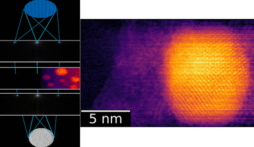
Atomic resolution imaging of light elements in electron-transparent materials has long been a challenge. Biomolecular materials, for example, are rapidly altered by incident electrons. We demonstrate a scanning transmission electron microscopy (STEM) technique, called STEM holography, capable of efficient structural analysis of beam-sensitive nanomaterials. STEM holography measures the absolute phase and amplitude of electrons passed through a specimen via interference with a vacuum reference wave. We use an amplitude-dividing nanofabricated grating to prepare multiple beams focused at the sample. We configure the postspecimen microscope imaging system to overlap the beams, forming an interference pattern. We record and analyze the pattern at each 2D-raster-scan-position, reconstructing the complex object wave. As a demonstration, we image gold nanoparticles on an amorphous carbon substrate at 2.4 Å resolution. STEM holography offers higher contrast of the carbon while maintaining gold atomic lattice resolution compared to high angle annular dark field STEM.
中文翻译:

以亚纳米分辨率探测光原子:扫描透射电子显微镜全息术的实现
长期以来,电子透明材料中轻元素的原子分辨率成像一直是一个挑战。例如,生物分子材料会被入射电子迅速改变。我们演示了一种称为STEM全息图的扫描透射电子显微镜(STEM)技术,该技术能够对射线敏感的纳米材料进行有效的结构分析。STEM全息术通过干扰真空基准波来测量通过样品的电子的绝对相位和振幅。我们使用分频的纳米加工光栅来准备聚焦在样品上的多束光束。我们将样本后显微镜成像系统配置为重叠光束,形成干涉图样。我们记录并分析每个2D光栅扫描位置处的模式,以重建复杂的对象波。作为示范,我们以2.4Å分辨率将金纳米颗粒成像在无定形碳基材上。与高角度环形暗场STEM相比,STEM全息术可提供更高的碳反差,同时保持金原子晶格分辨率。
更新日期:2018-09-28
中文翻译:
以亚纳米分辨率探测光原子:扫描透射电子显微镜全息术的实现
长期以来,电子透明材料中轻元素的原子分辨率成像一直是一个挑战。例如,生物分子材料会被入射电子迅速改变。我们演示了一种称为STEM全息图的扫描透射电子显微镜(STEM)技术,该技术能够对射线敏感的纳米材料进行有效的结构分析。STEM全息术通过干扰真空基准波来测量通过样品的电子的绝对相位和振幅。我们使用分频的纳米加工光栅来准备聚焦在样品上的多束光束。我们将样本后显微镜成像系统配置为重叠光束,形成干涉图样。我们记录并分析每个2D光栅扫描位置处的模式,以重建复杂的对象波。作为示范,我们以2.4Å分辨率将金纳米颗粒成像在无定形碳基材上。与高角度环形暗场STEM相比,STEM全息术可提供更高的碳反差,同时保持金原子晶格分辨率。


 京公网安备 11010802027423号