Our official English website, www.x-mol.net, welcomes your feedback! (Note: you will need to create a separate account there.)
Direct CVD Growth of Graphene on Technologically Important Dielectric and Semiconducting Substrates
Advanced Science ( IF 15.1 ) Pub Date : 2018-09-22 , DOI: 10.1002/advs.201800050 Afzal Khan 1 , Sk Masiul Islam 2, 3 , Shahzad Ahmed 4 , Rishi R Kumar 4 , Mohammad R Habib 5 , Kun Huang 1 , Ming Hu 1 , Xuegong Yu 1 , Deren Yang 1
Advanced Science ( IF 15.1 ) Pub Date : 2018-09-22 , DOI: 10.1002/advs.201800050 Afzal Khan 1 , Sk Masiul Islam 2, 3 , Shahzad Ahmed 4 , Rishi R Kumar 4 , Mohammad R Habib 5 , Kun Huang 1 , Ming Hu 1 , Xuegong Yu 1 , Deren Yang 1
Affiliation
|
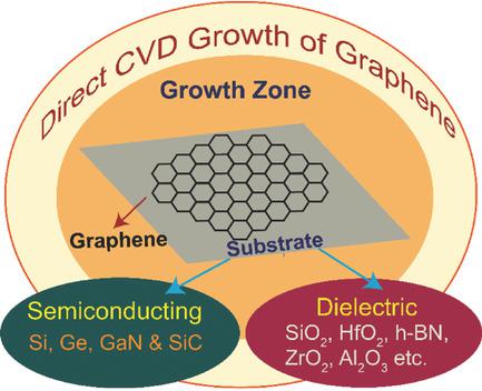
To fabricate graphene based electronic and optoelectronic devices, it is highly desirable to develop a variety of metal‐catalyst free chemical vapor deposition (CVD) techniques for direct synthesis of graphene on dielectric and semiconducting substrates. This will help to avoid metallic impurities, high costs, time consuming processes, and defect‐inducing graphene transfer processes. Direct CVD growth of graphene on dielectric substrates is usually difficult to accomplish due to their low surface energy. However, a low‐temperature plasma enhanced CVD technique could help to solve this problem. Here, the recent progress of metal‐catalyst free direct CVD growth of graphene on technologically important dielectric (SiO2, ZrO2, HfO2, h‐BN, Al2O3, Si3N4, quartz, MgO, SrTiO3, TiO2, etc.) and semiconducting (Si, Ge, GaN, and SiC) substrates is reviewed. High and low temperature direct CVD growth of graphene on these substrates including growth mechanism and morphology is discussed. Detailed discussions are also presented for Si and Ge substrates, which are necessary for next generation graphene/Si/Ge based hybrid electronic devices. Finally, the technology development of the metal‐catalyst free direct CVD growth of graphene on these substrates is concluded, with future outlooks.
中文翻译:

在技术上重要的介电和半导体基底上直接 CVD 生长石墨烯
为了制造基于石墨烯的电子和光电器件,非常需要开发各种无金属催化剂的化学气相沉积(CVD)技术,用于在介电和半导体基底上直接合成石墨烯。这将有助于避免金属杂质、高成本、耗时的过程以及引起缺陷的石墨烯转移过程。由于表面能较低,在介电基板上直接 CVD 生长石墨烯通常很难实现。然而,低温等离子体增强CVD技术可以帮助解决这个问题。这里,在技术上重要的电介质(SiO 2、ZrO 2、HfO 2、h-BN、Al 2 O 3、Si 3 N 4 、石英、MgO、SrTiO 3 、综述了TiO 2等)和半导体(Si、Ge、GaN 和 SiC)衬底。讨论了石墨烯在这些基底上的高温和低温直接 CVD 生长,包括生长机制和形态。还对 Si 和 Ge 衬底进行了详细讨论,这对于下一代基于石墨烯/Si/Ge 的混合电子器件是必需的。最后,总结了在这些基底上无金属催化剂直接 CVD 生长石墨烯的技术进展,并对未来进行了展望。
更新日期:2018-09-22
中文翻译:
在技术上重要的介电和半导体基底上直接 CVD 生长石墨烯
为了制造基于石墨烯的电子和光电器件,非常需要开发各种无金属催化剂的化学气相沉积(CVD)技术,用于在介电和半导体基底上直接合成石墨烯。这将有助于避免金属杂质、高成本、耗时的过程以及引起缺陷的石墨烯转移过程。由于表面能较低,在介电基板上直接 CVD 生长石墨烯通常很难实现。然而,低温等离子体增强CVD技术可以帮助解决这个问题。这里,在技术上重要的电介质(SiO 2、ZrO 2、HfO 2、h-BN、Al 2 O 3、Si 3 N 4 、石英、MgO、SrTiO 3 、综述了TiO 2等)和半导体(Si、Ge、GaN 和 SiC)衬底。讨论了石墨烯在这些基底上的高温和低温直接 CVD 生长,包括生长机制和形态。还对 Si 和 Ge 衬底进行了详细讨论,这对于下一代基于石墨烯/Si/Ge 的混合电子器件是必需的。最后,总结了在这些基底上无金属催化剂直接 CVD 生长石墨烯的技术进展,并对未来进行了展望。


 京公网安备 11010802027423号