Our official English website, www.x-mol.net, welcomes your feedback! (Note: you will need to create a separate account there.)
Photoresist Contact Patterning of Quantum Dot Films
ACS Nano ( IF 17.1 ) Pub Date : 2018-09-24 00:00:00 , DOI: 10.1021/acsnano.8b04462 Hohyun Keum 1 , Yiran Jiang 2 , Jun Kyu Park 1 , Joseph C. Flanagan 2 , Moonsub Shim 2 , Seok Kim 1
ACS Nano ( IF 17.1 ) Pub Date : 2018-09-24 00:00:00 , DOI: 10.1021/acsnano.8b04462 Hohyun Keum 1 , Yiran Jiang 2 , Jun Kyu Park 1 , Joseph C. Flanagan 2 , Moonsub Shim 2 , Seok Kim 1
Affiliation
|
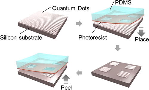
Scalable and cost-effective protocols to pattern and integrate colloidal quantum dots (QDs) with high resolution have been challenging to establish. While their solubility can facilitate certain processes such as spin-casting into thin films, it also makes them incompatible with many conventional patterning techniques including photolithography that require solution processing. In this work, we present “photoresist (PR) contact patterning”, a dry means to pattern QD films over large areas with high resolution while maintaining desired properties. Here, a PR layer on an elastomer substrate is patterned by conventional photolithography and used as a dry contact stamp to selectively peel off QDs in the contact regions, leaving behind a QD film with the negative of the PR pattern. Once patterned, QD films are readily transferred and integrated on foreign substrates by subsequent transfer printing processes. Patterned PR layers can also be transferred from elastomer substrates onto QD films and used as masking layers for subsequent deposition and patterning of additional materials, e.g., patterned metal electrodes or charge transport layers for QD-based devices. The study of the interfacial mechanics and energy of materials associated with PR contact patterning reveals why a lithographically patterned PR is superior for high-resolution QD film patterning. Applicability of PR contact patterning is demonstrated through the fabrication of red, green, and blue (RGB) QD light-emitting diode pixels. PR contact patterning presented in this work not only allows dry patterning of QD films but also enables high-resolution integration of functional multistack structures for future QD-based electronic and optoelectronic devices.
中文翻译:

量子点薄膜的光致抗蚀剂接触构图
建立具有高分辨率的模式化和集成胶体量子点(QD)的可扩展且具有成本效益的协议具有挑战性。尽管它们的溶解度可以促进某些工艺(例如旋铸成薄膜),但也使它们与许多传统的构图技术(包括需要溶液处理的光刻技术)不兼容。在这项工作中,我们提出“光致抗蚀剂(PR)接触图案”,这是一种干燥的方法,可以在较大的区域上以高分辨率将QD膜图案化,同时保持所需的性能。在此,弹性体基板上的PR层通过常规的光刻法被图案化并且用作干接触印模以选择性地剥离接触区域中的QD,从而留下具有PR图案的负片的QD膜。一旦图案化,QD膜易于通过后续的转移印刷工艺转移并整合到异物基材上。图案化的PR层也可以从弹性体基材转移到QD膜上,并用作掩膜层,用于随后沉积和图案化其他材料,e。例如,用于基于QD的设备的带图案的金属电极或电荷传输层。对与PR接触构图相关的材料的界面力学和能量的研究揭示了为什么光刻构图的PR优于高分辨率QD膜构图。通过制作红色,绿色和蓝色(RGB)QD发光二极管像素,证明了PR接触图案的适用性。在这项工作中提出的PR接触图案不仅可以对QD薄膜进行干式图案化,而且还可以对未来基于QD的电子和光电设备进行功能多叠层结构的高分辨率集成。
更新日期:2018-09-24
中文翻译:
量子点薄膜的光致抗蚀剂接触构图
建立具有高分辨率的模式化和集成胶体量子点(QD)的可扩展且具有成本效益的协议具有挑战性。尽管它们的溶解度可以促进某些工艺(例如旋铸成薄膜),但也使它们与许多传统的构图技术(包括需要溶液处理的光刻技术)不兼容。在这项工作中,我们提出“光致抗蚀剂(PR)接触图案”,这是一种干燥的方法,可以在较大的区域上以高分辨率将QD膜图案化,同时保持所需的性能。在此,弹性体基板上的PR层通过常规的光刻法被图案化并且用作干接触印模以选择性地剥离接触区域中的QD,从而留下具有PR图案的负片的QD膜。一旦图案化,QD膜易于通过后续的转移印刷工艺转移并整合到异物基材上。图案化的PR层也可以从弹性体基材转移到QD膜上,并用作掩膜层,用于随后沉积和图案化其他材料,e。例如,用于基于QD的设备的带图案的金属电极或电荷传输层。对与PR接触构图相关的材料的界面力学和能量的研究揭示了为什么光刻构图的PR优于高分辨率QD膜构图。通过制作红色,绿色和蓝色(RGB)QD发光二极管像素,证明了PR接触图案的适用性。在这项工作中提出的PR接触图案不仅可以对QD薄膜进行干式图案化,而且还可以对未来基于QD的电子和光电设备进行功能多叠层结构的高分辨率集成。


 京公网安备 11010802027423号