Our official English website, www.x-mol.net, welcomes your feedback! (Note: you will need to create a separate account there.)
Interfacial Electron Beam Lithography: Chemical Monolayer Nanopatterning via Electron-Beam-Induced Interfacial Solid-Phase Oxidation
ACS Nano ( IF 17.1 ) Pub Date : 2018-09-14 00:00:00 , DOI: 10.1021/acsnano.8b03416 Rivka Maoz 1 , Jonathan Berson 1 , Doron Burshtain 1 , Peter Nelson 1 , Ariel Zinger 1 , Ora Bitton 2 , Jacob Sagiv 1
ACS Nano ( IF 17.1 ) Pub Date : 2018-09-14 00:00:00 , DOI: 10.1021/acsnano.8b03416 Rivka Maoz 1 , Jonathan Berson 1 , Doron Burshtain 1 , Peter Nelson 1 , Ariel Zinger 1 , Ora Bitton 2 , Jacob Sagiv 1
Affiliation
|
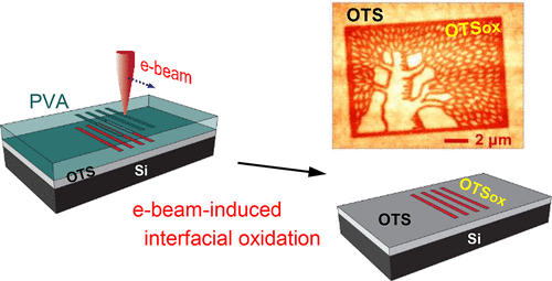
Chemical nanopatterning—the deliberate nanoscale modification of the chemical nature of a solid surface—is conveniently realized using organic monolayer coatings to impart well-defined chemical functionalities to selected surface regions of the coated solid. Most monolayer patterning methods, however, exploit destructive processes that introduce topographic as well as other undesired structural and chemical transformations along with the desired surface chemical modification. In particular in electron beam lithography (EBL), organic monolayers have been used mainly as ultrathin resists capable of improving the resolution of patterning via local deposition or removal of material. On the basis of the recent discovery of a class of radiation-induced interfacial chemical transformations confined to the contact surface between two solids, we have advanced a direct, nondestructive EBL approach to chemical nanopatterning—interfacial electron beam lithography (IEBL)—demonstrated here by the e-beam-induced local oxidation of the −CH3 surface moieties of a highly ordered self-assembled n-alkylsilane monolayer to −COOH while fully preserving the monolayer structural integrity and molecular organization. In this conceptually different EBL process, the traditional resist is replaced by a thin film coating that acts as a site-activated reagent/catalyst in the chemical modification of the coated surface, here the top surface of the to-be-patterned monolayer. Structural and chemical transformations induced in the thin film coating and the underlying monolayer upon exposure to the electron beam were elucidated using a semiquantitative surface characterization methodology that combines multimode AFM imaging with postpatterning surface chemical modifications and quantitative micro-FTIR measurements. IEBL offers attractive opportunities in chemical nanopatterning, for example, by enabling the application of the advanced EBL technology to the straightforward nanoscale functionalization of the simplest commonly used organosilane monolayers.
中文翻译:

界面电子束光刻:通过电子束诱导的界面固相氧化进行化学单层纳米构图
化学纳米图案-固体表面化学性质的刻意的纳米级修饰-使用有机单层涂层方便地实现,可以为涂覆的固体的选定表面区域赋予定义明确的化学功能。然而,大多数单层图案化方法利用破坏性过程,该破坏性过程引入了形貌以及其他不期望的结构和化学转变以及所需的表面化学改性。尤其是在电子束光刻(EBL)中,有机单层主要用作能够改善图形化分辨率的超薄抗蚀剂。材料的局部沉积或去除。根据最近发现的一类辐射诱导的界面化学转变限制在两种固体之间的接触表面的基础上,我们提出了一种直接的,无损的EBL方法进行化学纳米图案化-界面电子束光刻(IEBL),在此进行了演示电子束诱导的高度有序自组装n -CH 3表面部分的局部氧化-烷基硅烷单层成-COOH,同时充分保留单层的结构完整性和分子结构。在这种概念上不同的EBL工艺中,传统的抗蚀剂被薄膜涂层代替,该薄膜涂层在涂层表面(此处是待图案化的单层的上表面)的化学改性中充当位活化试剂/催化剂。使用半定量表面表征方法阐明了薄膜涂层和下层单层在电子束曝光后引起的结构和化学转化,该方法将多模AFM成像与后图案化表面化学修饰和定量micro-FTIR测量相结合。IEBL在化学纳米图案化方面提供了诱人的机会,例如,
更新日期:2018-09-14
中文翻译:
界面电子束光刻:通过电子束诱导的界面固相氧化进行化学单层纳米构图
化学纳米图案-固体表面化学性质的刻意的纳米级修饰-使用有机单层涂层方便地实现,可以为涂覆的固体的选定表面区域赋予定义明确的化学功能。然而,大多数单层图案化方法利用破坏性过程,该破坏性过程引入了形貌以及其他不期望的结构和化学转变以及所需的表面化学改性。尤其是在电子束光刻(EBL)中,有机单层主要用作能够改善图形化分辨率的超薄抗蚀剂。材料的局部沉积或去除。根据最近发现的一类辐射诱导的界面化学转变限制在两种固体之间的接触表面的基础上,我们提出了一种直接的,无损的EBL方法进行化学纳米图案化-界面电子束光刻(IEBL),在此进行了演示电子束诱导的高度有序自组装n -CH 3表面部分的局部氧化-烷基硅烷单层成-COOH,同时充分保留单层的结构完整性和分子结构。在这种概念上不同的EBL工艺中,传统的抗蚀剂被薄膜涂层代替,该薄膜涂层在涂层表面(此处是待图案化的单层的上表面)的化学改性中充当位活化试剂/催化剂。使用半定量表面表征方法阐明了薄膜涂层和下层单层在电子束曝光后引起的结构和化学转化,该方法将多模AFM成像与后图案化表面化学修饰和定量micro-FTIR测量相结合。IEBL在化学纳米图案化方面提供了诱人的机会,例如,


 京公网安备 11010802027423号